Thin film transistor and active matrix type display unit production methods therefor

Inactive Publication Date: 2006-02-07
SANYO ELECTRIC CO LTD
View PDF19 Cites 22 Cited by
  • Summary
  • Abstract
  • Description
  • Claims
  • Application Information

AI Technical Summary

Benefits of technology

[0057]As described above, the step of doping impurities of a first conductivity type, especially the high concentration impurity doping step, is performed prior to the step of forming a gate insulating film, and impurities are directly doped to an active layer of the transistor. As a result, acceleration energy of doped impurities can be lowered to the level just enough to reach a predetermined depth of the active layer. When the acceleration energy of the impurity ions is small, a resist mask is prevented from curing even in an environment in which impurities are doped at a high concentration, and can be completely removed after the doping step. Further, at the step of doping impurities of the other conductivity type (impurities of the second conductivity type), the active layer is masked with a material layer for its gate electrode. As described above, the gate electrode material layer does not lead to the problem of curing,

Problems solved by technology

Thus, etching adjustment is difficult and errors in depth or siz

Method used


Image

  • Thin film transistor and active matrix type display unit production methods therefor
  • Thin film transistor and active matrix type display unit production methods therefor
  • Thin film transistor and active matrix type display unit production methods therefor

Examples


Example

First Embodiment

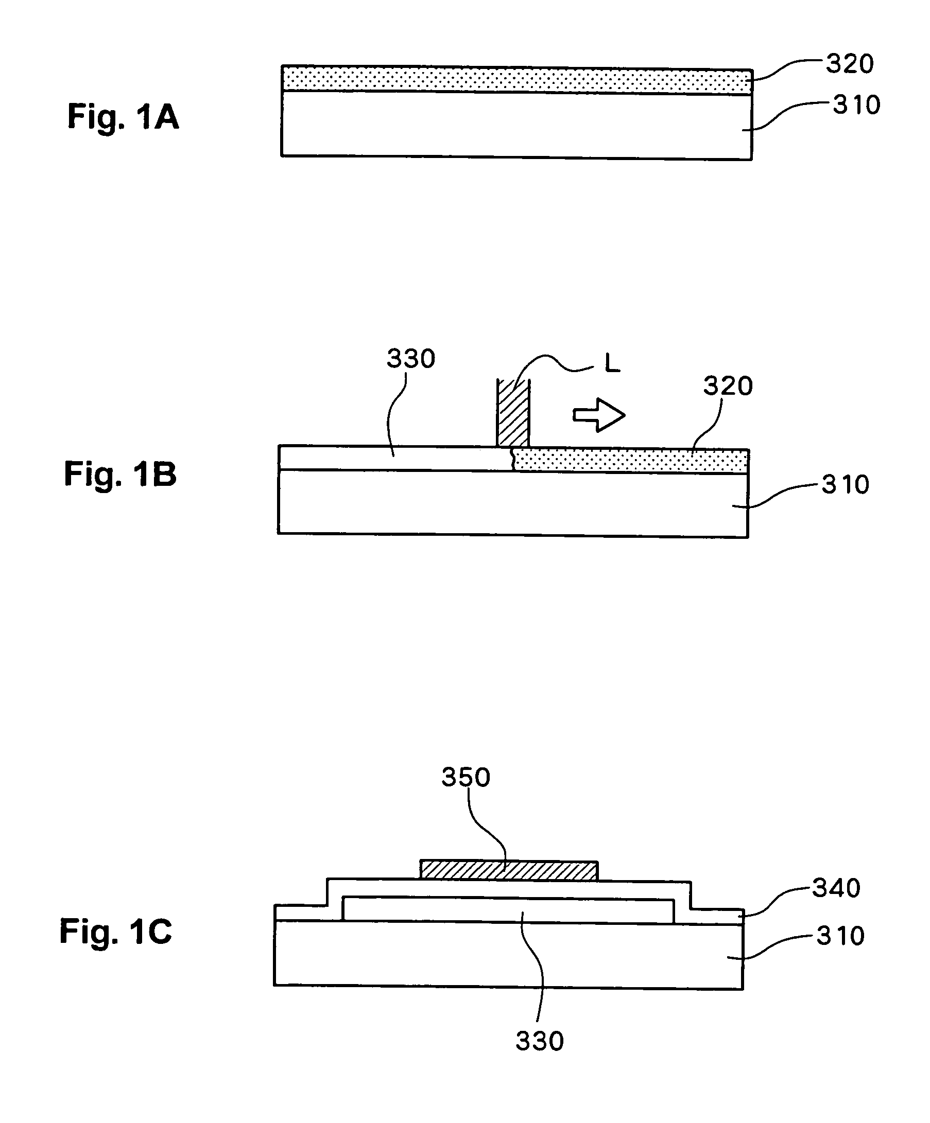
[0073]FIGS. 2A–2M, and FIG. 3 illustrate a method of manufacturing an active matrix display device according to a first embodiment of the present invention.

[0074]Step 1 (FIG. 2A): Over the entire surface of an insulating substrate 1 of quartz, non-alkaline glass, or the like, an a-Si film 2 is formed by plasma CVD (chemical vapor deposition) using gas including SH4 (silane), Si2H6 (disilane), or the like.

[0075]Step 2 (FIG. 2B): The surface of the a-Si film 2 is irradiated with a laser beam L for annealing, thereby melting and recrystallizing a-Si to form a poli-Si semiconductor film 3. Because the grain size of poli-Si according to the laser irradiation energy density and the number of times a laser is irradiated, the energy density of the laser beam L is optimized to provide the maximum grain size.

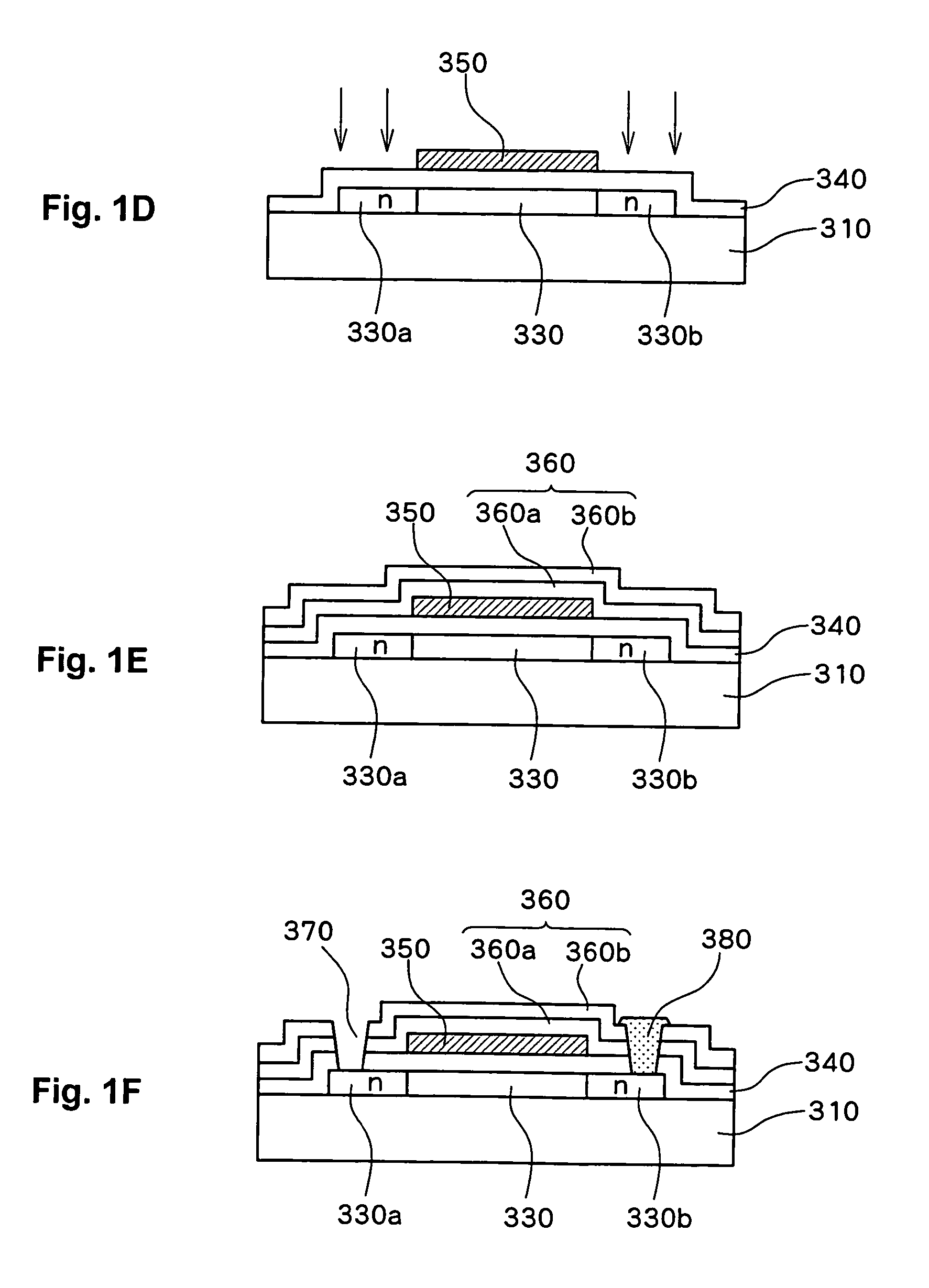
[0076]Step 3 (FIG. 2C): A photoresist film is formed on the semiconductor film 3 for light exposure. The portion of the photoresist film exposed to light is removed, leavi...

Example

Second Embodiment

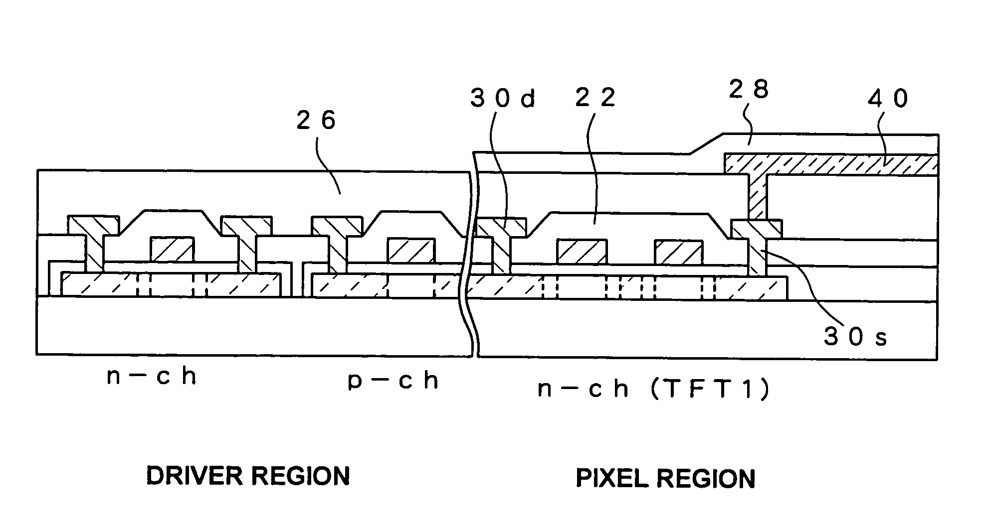
[0092]A second embodiment will next be described. FIG. 4 is a cross sectional view of a TFT substrate formed by manufacturing steps according to the second embodiment. The steps up to Step 7 are the same as those in the first embodiment illustrated in FIGS. 2A–2G, and therefore description thereof will not be repeated.

[0093]Step 8: Through photolithography and etching, a second contact hole 9 (9d) is formed penetrating the interlayer insulating film 8 and exposing the first contact 7d.

[0094]Step 9: On the interlayer insulating film 8 and the second contact hole, a metal film in thickness of 3000 Å is formed as a second conductive film by sputtering, to form wiring 13d extending in a direction perpendicular to the plane of the sheet in the second contact hole by photolithography and etching.

[0095]Step 10: The planarization film 26 is formed covering the interlayer insulating film 8 and the wiring 13d.

[0096]Step 11: Through photolithography and etching, a third cont...

Example

[0100]A third embodiment, in which the number of first contacts for each TFT is different from those in the above-described first and second embodiments, will next be described. FIGS. 5 and 6 are cross sectional views of the TFT substrate formed by manufacturing steps according to the third embodiment. The manufacturing steps up to Step 4 are the same as those in the first embodiment illustrated in FIGS. 2A–2D, and therefore description thereof will not be repeated.

[0101]Step 5: Through photolithography and etching, only the first contact hole 6s is formed penetrating the gate insulating film 5 and exposing part of the source region 3s illustrated in FIG. 2E.

[0102]Step 6: On the gate insulating film 5 and the first contact hole, a metal film is formed as a first conductive film in thickness of 2000 Å by sputtering. Through photolithography and etching, the gate electrode 7g is formed on the region of the gate insulating film 5 corresponding to and located on the channel region 3ch. ...


PUM


Abstract

A first contact hole is formed penetrating a gate insulating film, on which a gate electrode is formed and simultaneously a first contact is formed in the first contact hole. A second contact hole penetrating an interlayer insulating film is formed, and a second contact is formed in the second contact hole. A third contact hole is formed penetrating a planarization film, and an electrode is formed in the third contact hole. By using a plurality of contact holes for electrically connecting the electrode and a semiconductor film, the aspect ratio of each contact hole can be reduced, thereby achieving improvement in yield, high-level integration due to a reduction in difference in area between upper and bottom surfaces of the contact, and other advantageous improvements.

Description

TECHNICAL FIELD[0001]The present invention relates to a thin film transistor (hereinafter referred to as a TFT) and an active matrix display device including the TFT, and a manufacturing method thereof.BACKGROUND ART[0002]Active matrix display devices in which a switching element is formed for each pixel to achieve a high-definition display in liquid crystal display devices are publicly known and organic electroluminescence display devices have recently attracted a great deal of attention.[0003]FIGS. 1A–1I are cross sectional views illustrating the steps of manufacturing an active matrix liquid crystal display device according to a related art.[0004]Step A (FIG. 1A): On an insulating substrate 310, an amorphous silicon (hereinafter referred to as “a-Si”) film 320 is formed.[0005]Step B (FIG. 1B): A surface of the a-Si film 320 is irradiated with beams of focused laser light (laser beams) to melt and recrystallize a-Si, thereby forming a polysilicon (hereinafter referred to as “poli-...

Claims


Application Information

Patent Timeline
IPC IPC(8): H01L21/00H01L21/84G02F1/1362H01L21/336H01L21/77H01L27/12H01L29/417H01L29/786
CPCG02F1/136227H01L27/1214H01L27/1288H01L29/66757H01L29/78621H01L29/41733G02F1/13454H01L27/124H01L29/786H01L27/127
Inventor YONEDA, KIYOSHIYAMADA, TSUTOMUYUDA, SHINJISUZUKI, KOJI
Owner SANYO ELECTRIC CO LTD
Why Eureka
Try Eureka