Display device with organic conductive thin film having conductive network

Active Publication Date: 2006-02-07
PANASONIC CORP
View PDF3 Cites 17 Cited by
  • Summary
  • Abstract
  • Description
  • Claims
  • Application Information

AI Technical Summary

Benefits of technology

[0009]Accordingly, it is an object of the present invention to provide an organic electronic device that enables high integration and high-speed response, a method of producing this organic electronic device, and a method of operating this organic electroni

Problems solved by technology

However, with reduction in the size of silicon crystals (to 0.1 μm or less), defects in the silicon have emerged, a shortcoming as the performance of a device is controlled by the crystallinity of the silicon.
Regarding the orga

Method used


Image

  • Display device with organic conductive thin film having conductive network
  • Display device with organic conductive thin film having conductive network
  • Display device with organic conductive thin film having conductive network

Examples


embodiment 1

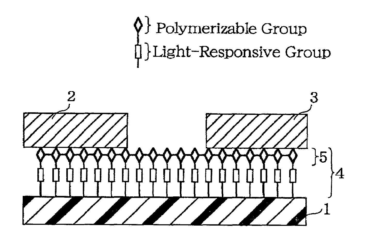
[0225]The present embodiment relates to an example of a two-terminal organic electronic device of the present invention. It is described with reference to FIG. 1.

[0226]This two-terminal organic electronic device is composed of, formed on a substrate 1, a first electrode 2, a second electrode 3, and a conductive organic thin film 4 contacting and being electrically connected to a portion of the undersurfaces of both electrodes. The conductive organic thin film 4 has a conductive network 5 in which organic molecules each having a light-responsive group and a polymerizable group are linked together.

[0227]Other than the requirement of having a light-responsive group and a polymerizable group, the organic molecules used in forming the conductive organic thin film 4 do not have any particular limitations, but among the many possibilities, it is suitable to use an organic molecule represented by the general formula (1) below (a silane-based chemisorbable substance):

A-(CH2)m-B-(CH2)n-SiDpE3...

embodiment 2

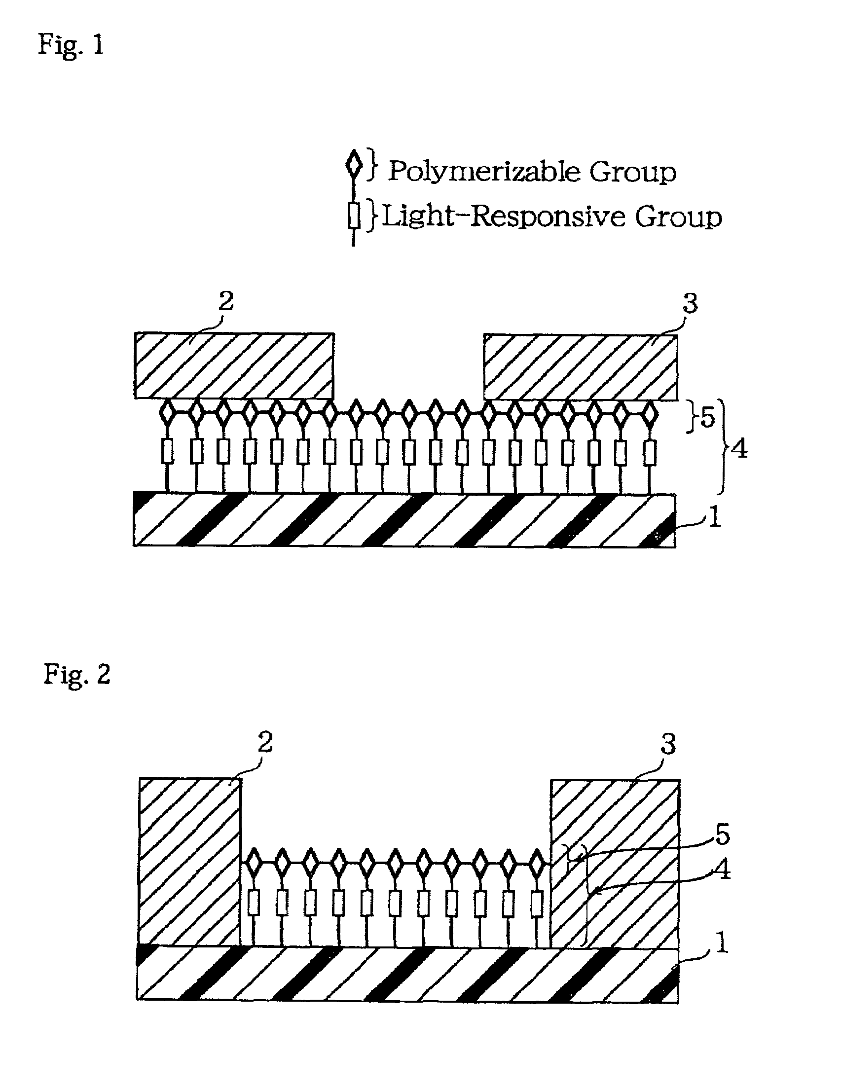
[0238]The present embodiment relates to another example of a two-terminal organic electronic device of the present invention. It is described with reference to FIG. 2.

[0239]This two-terminal organic electronic device is composed of, formed on a substrate 1, a first electrode 2, a second electrode 3, and a conductive organic thin film 4 contacting and being electrically connected to side surfaces of both electrodes. The conductive organic thin film 4 has a conductive network 5 in which organic molecules each having a light-responsive group and a polymerizable group are linked together.

[0240]The two-terminal organic electronic device of the present embodiment can be produced in the following manner. First, an insulating substrate or an insulating film-covered substrate that is an insulating film formed on a surface of an arbitrary substrate is prepared, and an organic thin film comprising the above-described organic molecules is formed using a photoresist or the like (step of forming ...

embodiment 3

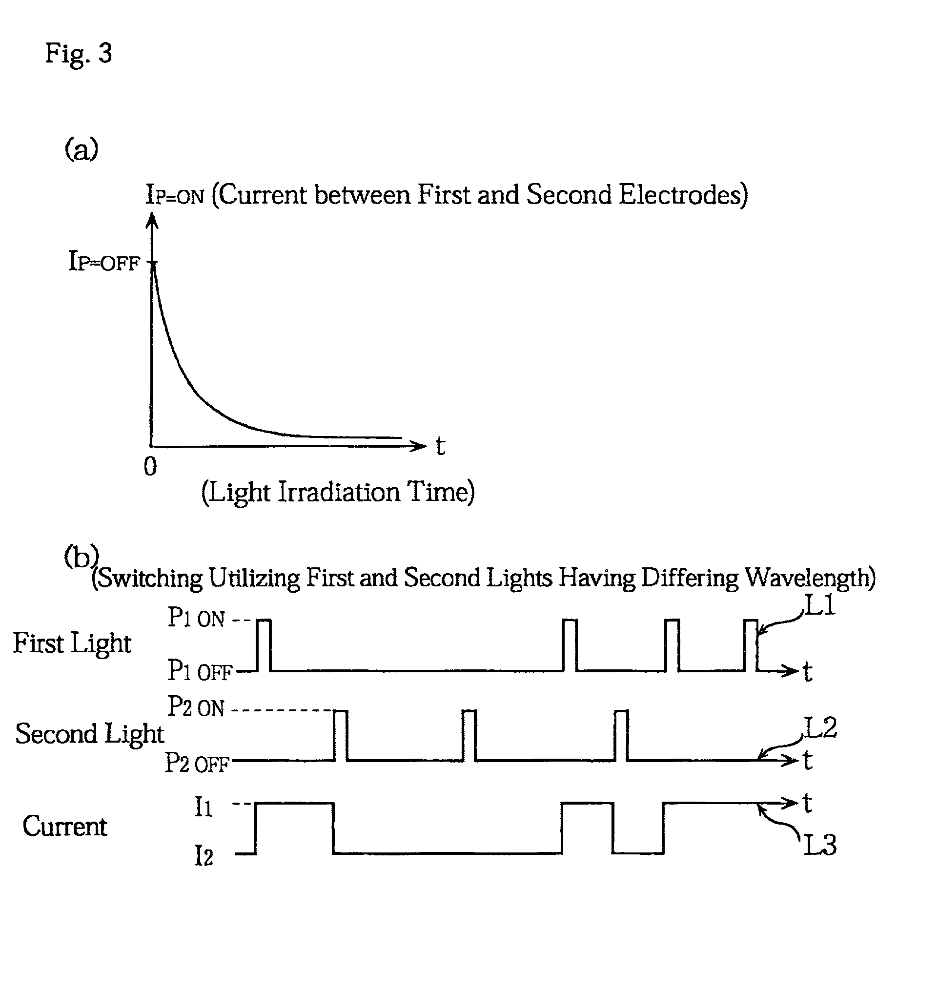
[0244]The present embodiment relates to a method of operating a two-terminal organic electronic device. Change in conductivity over time caused by light irradiation and the switching operations of a two-terminal organic electronic device are described with reference to FIG. 3.

[0245]FIG. 3(a) is schematic graph qualitatively showing change in conductivity as a function of irradiation time when the conductive organic thin film is irradiated with light of a constant intensity.

[0246]Considering that the amount of irradiated light is proportional to the product of the intensity of the irradiated light and irradiation time, the results are the same whether the amount of light with which the conductive organic thin film is irradiated, the irradiation time under the condition of constant light intensity, or the light intensity under the condition of constant irradiation time is plotted on the horizontal axis. In the following, the case in which the intensity of light is constant is describe...


PUM

PropertyMeasurementUnit
Electrical conductivityaaaaaaaaaa
Electrical conductoraaaaaaaaaa
Responsivityaaaaaaaaaa

Abstract

An organic electronic device is provided that utilizes a conductive organic thin film having a conductive network in the channel region. The conductive network comprises an organic molecular group made up of organic molecules each having a light-responsive group or a polar group bonded together by conjugated bonds. Thus, high integration and high-speed response is made possible. In addition, a method of producing a functional organic thin film fixed to a specified portion of a substrate surface by covalent bonds is provided. This method comprises preliminarily treating the substrate by performing an active hydrogen exposure treatment on the specified portion (or an active hydrogen removing treatment on the portion other than the specified portion) and reacting the active hydrogens of the specified portion with organic molecules. Thus, a high precision functional organic thin film, even one formed to the micron pattern level, can be provided.

Description

BACKGROUND OF THE INVENTION[0001](1) Field of the Invention[0002]The present invention relates to a two-terminal organic electronic device and a three-terminal organic electronic device (hereinafter referred to together as organic electronic devices), methods of producing the devices, and methods of operating the devices, both organic electronic devices being such that an organic material is used in the channel region. The present invention also relates to a liquid crystal display device and an electroluminescent display device hereinafter referred to as EL display device) and to methods of producing the display devices, both display devices utilizing the organic electronic devices.[0003]Furthermore, the present invention relates to a method of producing a functional organic thin film fixed to a substrate by covalent bonds, another method of producing an organic electronic device, and methods of producing a liquid crystal display device and an EL display device, both devices using t...

Claims


Application Information

Patent Timeline
IPC IPC(8): H05B33/00H01L27/32H01L51/00H01L51/30H01L51/40
CPCB82Y10/00H01L51/0035H01L51/0036H01L51/0052H01L51/0067H01L51/0068H01L51/0094H01L51/0508H01L51/0545H01L51/42H01L51/428H01L27/3274Y02E10/549H01L51/0006H01L51/004H01L51/0044H01L51/0075H01L51/0595H10K59/125H10K71/125H10K85/111H10K85/113H10K85/141H10K85/154H10K85/655H10K85/615H10K85/701H10K85/654H10K85/40H10K10/46H10K10/466H10K10/701H10K30/00H10K30/65E01H5/063
Inventor OGAWA, KAZUFUMI
Owner PANASONIC CORP
Why Eureka
Try Eureka