Semiconductor memory device including reference memory cell and control method

a memory cell and memory technology, applied in semiconductor devices, digital storage, instruments, etc., can solve the problems of uncertainty in the reliability of reference signals, methods that are sometimes unsuitable for memory cell arrays,

Inactive Publication Date: 2006-02-14
KK TOSHIBA
View PDF6 Cites 23 Cited by
  • Summary
  • Abstract
  • Description
  • Claims
  • Application Information

AI Technical Summary

Problems solved by technology

Therefore, the method is sometimes unsuitable for a memory cell array which has a large capacity since the method doesn't shows good scalability.
Therefore, there has been a tendency that the reliability of the reference signal has uncertainty.

Method used


Image

  • Semiconductor memory device including reference memory cell and control method
  • Semiconductor memory device including reference memory cell and control method
  • Semiconductor memory device including reference memory cell and control method

Examples


first embodiment

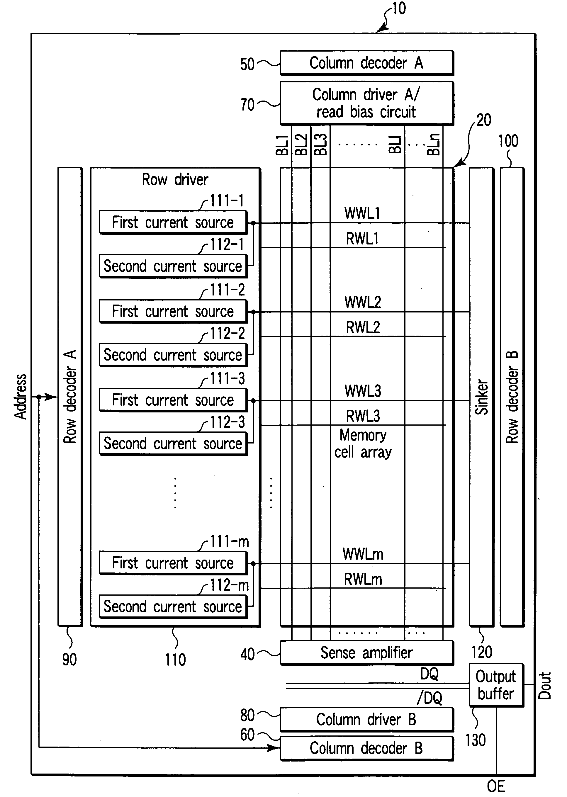
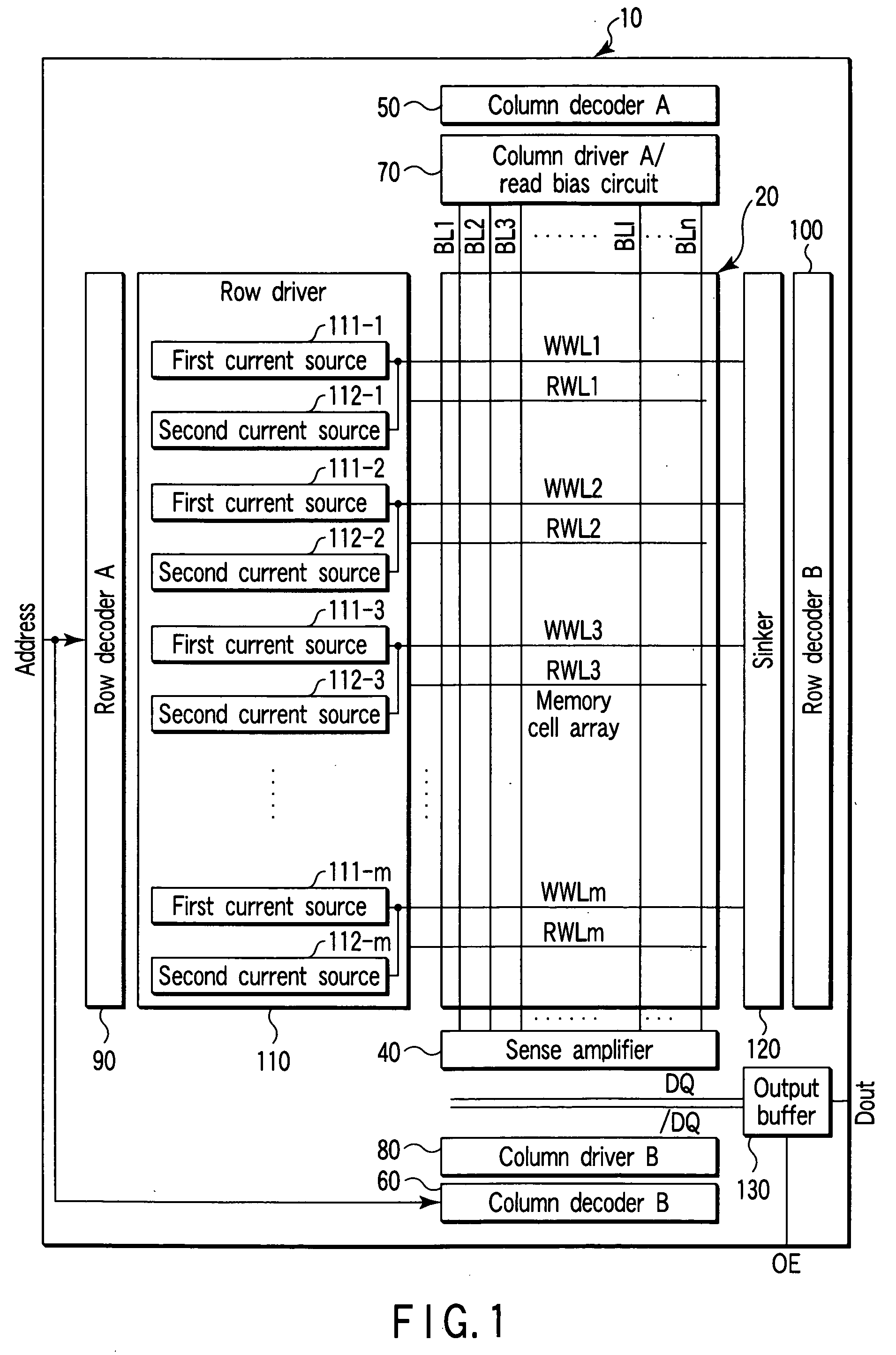
[0042]A semiconductor memory device according to the present invention will be described with reference to FIG. 1. FIG. 1 is a block diagram of MRAM according to the present embodiment.

[0043]As shown, a MRAM 10 includes a memory cell array 20, sense amplifier 40, column decoder A 50, column decoder B 60, column driver A / read bias circuit 70, column driver B 80, row decoder A 90, row decoder B 100, row driver 110, sinker 120, and output buffer 130.

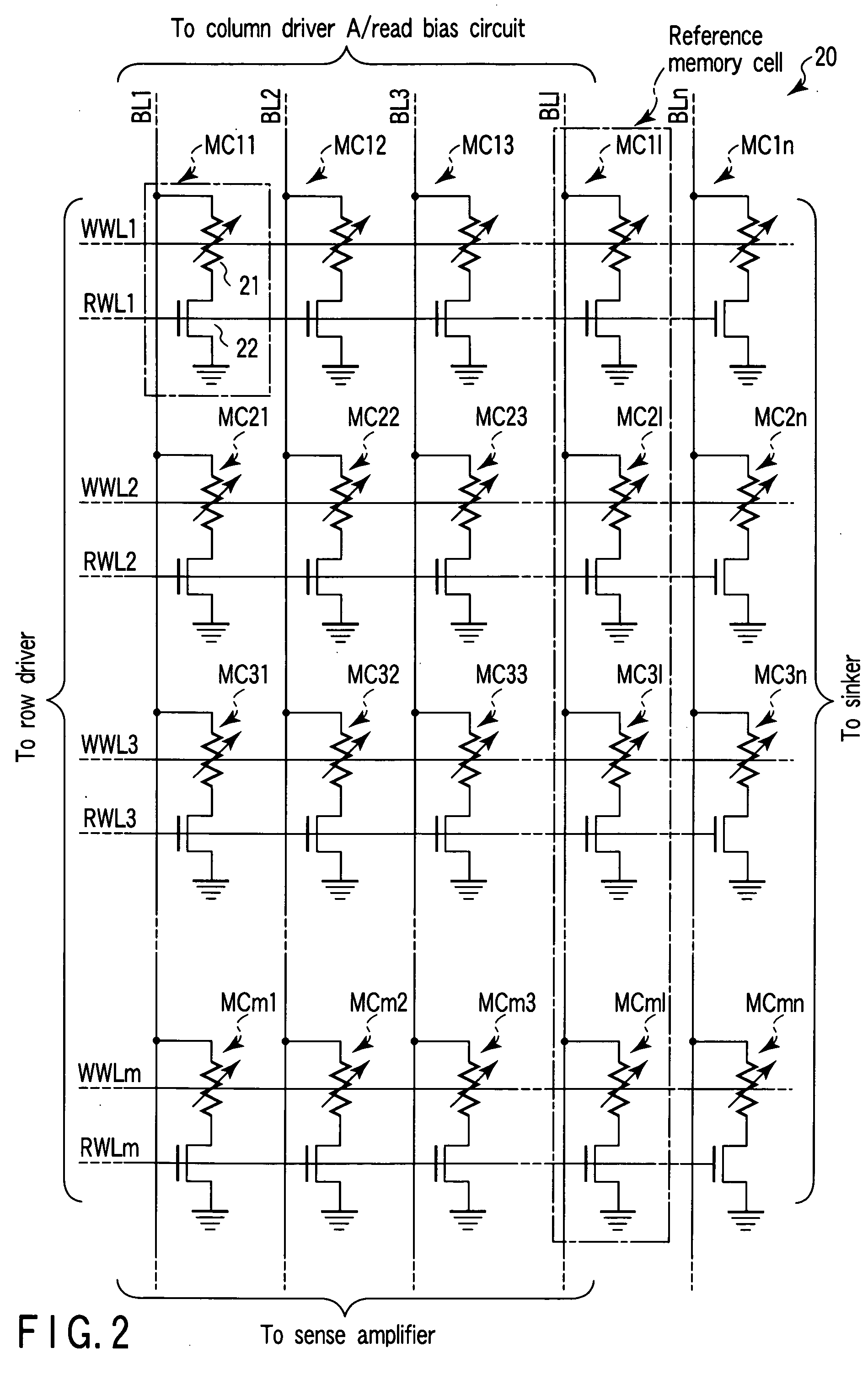
[0044]In the memory cell array 20, write word lines WWL1 to WWLm (m: natural number) and read word lines RWL1 to RWLm are formed along a predetermined direction (first direction), and bit lines BL1 to BLn (n: natural number) are formed along a direction (second direction) crossing at right angles to the first direction. One end of the write word lines WWL1 to WWLm and read word lines RWL1 to RWLm is connected to the row driver 110, and the other end of the write word lines WWL1 to WWLm is connected to the sinker 120. Moreover, one end of th...

second embodiment

[0109]The semiconductor memory device according to the invention will be described with reference to FIG. 9. FIG. 9 is a block diagram of the MRAM according to the present embodiment.

[0110]As FIG. 9 shows, this MRAM is identical to the first embodiment illustrated in FIG. 1, except that it comprises a control circuit 140 and fuse group 150. The components other than the circuit 140 and fuse group 150 will not described.

[0111]The control circuit 140 and fuse group 150 will be described, together with a method of generating reference signals, with reference to FIG. 10. FIG. 10 is a flowchart explaining the method of generating reference signals.

[0112]First, a semiconductor chip has been manufactured (step S1), the die sort test (step S2) is performed. At the die sort time, as described above in the first embodiment, the data is written in the reference memory cells MC1l to MCml (step S3). That is, the method comprises: adjusting the value of the write current Iw1 supplied to the write...


PUM


Abstract

A semiconductor memory device includes word lines, bit lines, first memory cells, second memory cells, a memory cell array, a row decoder, a row driver, a column decoder, a column driver, and a sense amplifier. The first memory cell includes a magneto-resistive element which has either a first resistance or a second resistance smaller than the first resistance. The second memory cell includes a magneto-resistive element which has a resistance between the first and second resistances. The memory cell array includes the first and second memory cells disposed in intersections of the word line and bit line. The row driver supplies a first write current to the word line. The column driver supplies a second write current to the bit line. The sense amplifier amplifies data read from the first memory cell.

Description

CROSS-REFERENCE TO RELATED APPLICATIONS[0001]This application is based upon and claims the benefit of priority from the prior Japanese Patent Application No. 2003-067901, filed Mar. 13, 2003, the entire contents of which are incorporated herein by reference.BACKGROUND OF THE INVENTION[0002]1. Field of the Invention[0003]The present invention relates to a semiconductor memory device and control method, for example, to a read operation of a magneto-resistive random access memory (MRAM).[0004]2. Description of the Related Art[0005]The MRAM is a device which uses a magneto-resistive effect to store “1” or “0” information and to perform a memory operation. Moreover, the device has a nonvolatile property, high integration property, and high reliability, also performs a high-speed operation, and is expected as a memory device which can replace to a related-art dynamic random access memory (DRAM) and electrically erasable and programmable read only memory (EEPROM).[0006]In the MRAM, a magne...

Claims


Application Information

Patent Timeline
Patent Type & Authority Patents(United States)
IPC IPC(8): G11C11/00G11C11/15G11C29/04H01L21/8246H01L27/105H01L43/08
CPCG11C11/15
Inventor SHIMIZU, YUUI
Owner KK TOSHIBA
Why Eureka
Try Eureka