High temperature superconducting josephson junctin, superconducting electronic device provided with the former and method of manufacturing high temperature superconducting josephson junction

a superconducting electronic device and high temperature technology, applied in the direction of superconducting magnets/coils, superconductor devices, magnetic bodies, etc., can solve the problems of short circuit in the junction, failure to meet the requirements of the combination described above, and the inability to obtain satisfactory i-v characteristics of the junction, etc., to achieve good, easy to form the thin superconductor film, and increase the margin of error

Inactive Publication Date: 2006-02-14
INT SUPERCONDUCTIVITY TECH CENT
View PDF11 Cites 13 Cited by
  • Summary
  • Abstract
  • Description
  • Claims
  • Application Information

AI Technical Summary

Benefits of technology

[0096]In the second aspect of the present invention, it is preferable that the two superconductor layers each include five elements and have compositions different from each other. This increases the margins of error for the process conditions that allow it to form a c-axis orientation film that is good in all respects including superconductivity, surface flatness and crystallinity, thus mak

Problems solved by technology

As a result, it can easily be anticipated that failure to satisfactorily perform as a Josephson junction may occur frequently as the junction layer becomes unacceptably thinner due to minor fluctuations in the process conditions during the formation of the junction that is carried out under very sensitive conditions, resulting in short circuiting in the junction.
However, satisfactory I-V characteristic of the junction could not necessarily be obtained from the combinations described above.
However, a physical film forming process such as sputtering process or laser deposition process does not offer process conditions having large margins that allow it to form a c-axis orientation film that is good in all respects including superconductivity, surface flatness and crystallinity, which are related to achieving high quality of superconductor film.
Therefore, it is a very tedious task to find out the optimum film forming conditions for both the second superconductor and the first superconductor.
Furthermore, operating conditions of thin film manufacturing apparatuses may differ from one apparatus to another, and there may be cases in which proper conditions for forming a c-axis orientation film of high quality cannot be found for the two superconductor materials that have been selected.
Thus, it is difficult to obtain a product having high performance and high reliability, even in the case of a Josephson junction formed by using the sam

Method used


Image

  • High temperature superconducting josephson junctin, superconducting electronic device provided with the former and method of manufacturing high temperature superconducting josephson junction
  • High temperature superconducting josephson junctin, superconducting electronic device provided with the former and method of manufacturing high temperature superconducting josephson junction
  • High temperature superconducting josephson junctin, superconducting electronic device provided with the former and method of manufacturing high temperature superconducting josephson junction

Examples


specific example 1

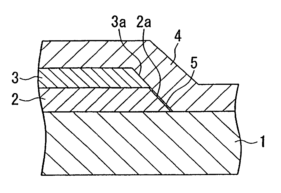
[0106]FIG. 1 is a sectional view of a high temperature superconducting Josephson junction of the ramp-edge type according to a first embodiment of the present invention. In the drawing, reference numeral 1 denotes a substrate, 2 denotes a first superconductor, 3 denotes an inter-layer insulation film, 4 denotes a second superconductor and 5 denotes a barrier layer.

[0107]The first superconductor 2 is processed at an edge thereof so as to form an edge face 2a inclined by a predetermined angle from the surface of the substrate 1.

[0108]Similarly to the first superconductor 2, the inter-layer insulation film 3 is also processed to form an edge face inclined against the substrate 1, namely, an edge face 3a lying in the same plane as the edge face 2a of the first superconductor 2.

[0109]The second superconductor 4 is formed so as to cover the first superconductor 2 and the inter-layer insulation film 3 as a whole in the Josephson junction. An extremely thin barrier layer 5 is formed in the ...

specific example 2

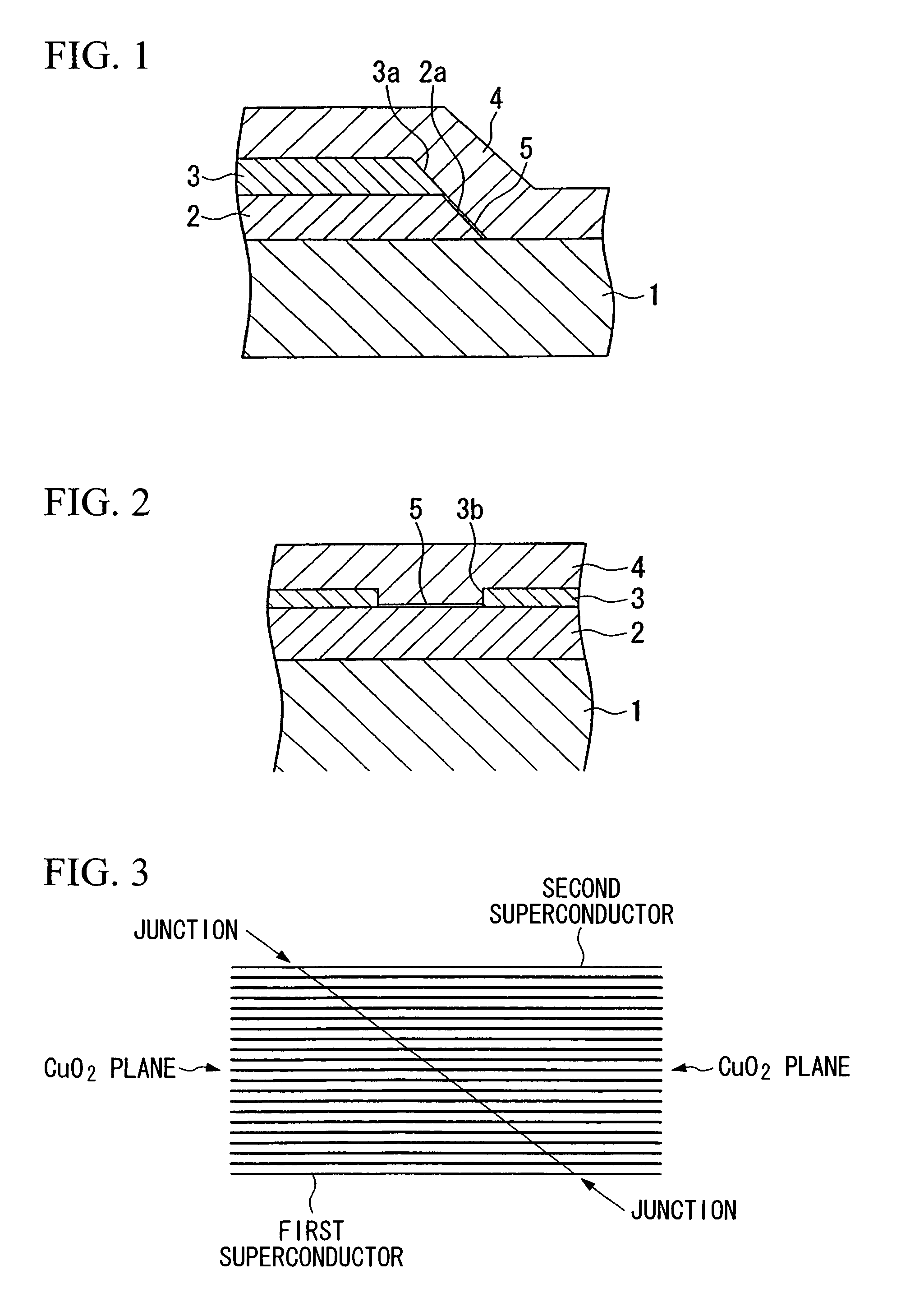
[0132]FIG. 2 is a sectional view of the stacked type high temperature superconducting Josephson junction according to the second embodiment of the present invention. The first superconductor 2 and the inter-layer insulation film 3 are formed successively on the substrate 1, the opening 3b is formed in the inter-layer insulation film 3 at a position where a Josephson junction is to be made, the second superconductor 4 is formed on the inter-layer insulation film 3 and on the first superconductor 2 that is exposed through the opening 3b, and the damaged layer produced by bombarding Ar ions (Ar+) on the surface of the first superconductor 2 that is exposed through the opening 3b reacts with the first superconductor 2 and the second superconductor 4 so as to turn into the extremely thin barrier layer 5.

[0133]Thus, the Josephson junction of this embodiment has a structure different from that of the Josephson junction of the first embodiment described previously.

[0134]The Josephson juncti...

example 1

[0137]In this example, the Josephson junction is of an IEJ type wherein the layer damaged during processing is used as the junction, as shown in FIG. 1, while formation of such a ramp-edge type Josephson junction was attempted as the variance (σ / X) was restrained within 10% and critical current Ic is 1.0 mA or higher (4.2K). 25 Pieces of the device were made for each test.

[0138]As examples of the prior art, devices having the first superconductor and the second superconductor made of YBa2Cu3Oy (hereinafter, y that represents the proportion of oxygen atoms in the formula takes a value that satisfies the requirement of the formula concerning the valence) were manufactured.

[0139](La,Sr)2AlTaO6 (LSAT) (100) was used for the substrate over which YBa2Cu3Oy film was formed to a thickness of 200 nm by off-axis high frequency sputtering process for the first superconductor.

[0140]A c-axis orientation film having a flat surface was formed by setting the substrate temperature to 750° C., high f...


PUM

PropertyMeasurementUnit
Fractionaaaaaaaaaa
Radiusaaaaaaaaaa
Temperatureaaaaaaaaaa

Abstract

A Josephson junction having a barrier layer sandwiched by two superconductors wherein the superconductors include one or more elements selected from the group of Y, La, Nd, Sm, Eu, Gd, Dy, Ho, Er, Tm, Yb and Lu, one or more elements selected from the group of Ba, Sr and Ca, and Cu and oxygen, wherein the two superconductors each include at least five elements with compositions different from each other, or the barrier layer (5) includes one or more elements selected from the group of La, Nd, Sm and Eu, and one or more elements selected from the group of Y, Gd, Dy, Ho, Er, Tm, Yb and Lu.

Description

TECHNICAL FIELD[0001]The present invention relates to a high temperature superconducting Josephson junction, a superconducting electronic device provided with the high temperature superconducting Josephson junction, and a method of manufacturing the high temperature superconducting Josephson junction.BACKGROUND ART[0002]A superconductor with unique properties such as (1) having zero electric resistance, (2) being perfect diamagnet and (3) exhibiting the Josephson effect, is expected to have wide applications including transmission of electric power, generation of electric power, confinement of plasma for nuclear fusion, magnetically levitated vehicles, magnetic shields, ultra-high sensitivity magnetic sensors, high-speed microwave communication devices and high-speed computers.[0003]In the past, known superconductors were only those having low superconducting transition temperatures (Tc) such as NbTi and Nb3Sn. In 1986, Bednorz and Mueller discovered a copper oxide high temperature ...

Claims


Application Information

Patent Timeline
IPC IPC(8): H01L23/48H01B12/00H01L27/00H01L29/00H01L39/22H01L39/24
CPCH01L39/225H01L39/2496H01L2924/0002H01L2924/00H10N60/124H10N60/0941H10N60/10
Inventor ADACHI, SEIJIWAKANA, HIRONORITANABE, KEIICHI
Owner INT SUPERCONDUCTIVITY TECH CENT
Why Eureka
Try Eureka