Linear associative memory-based hardware architecture for fault tolerant ASIC/FPGA work-around

a hardware architecture and associative memory technology, applied in the field of electronic circuits, can solve the problems of inability to guarantee 100% coverage, most time-consuming and complicated approaches, and fpga is usually larger and more complex than a pld

Inactive Publication Date: 2006-02-14
CISCO TECH INC
View PDF8 Cites 56 Cited by
  • Summary
  • Abstract
  • Description
  • Claims
  • Application Information

AI Technical Summary

Benefits of technology

[0018]It is yet another object of the present invention to provide a fault-tolerant ASIC / FPGA which can identify potentially bad input vectors from a faulty block and handle those bad vectors using a software work-around, while still using the faulty block for good vectors.

Problems solved by technology

ASICs can be built using customized circuits at every level, which is the most time-consuming and complicated approach, or be built using gate arrays, standard cells, or programmable logic devices.
An FPGA is usually larger and more complex than a PLD.
This scheme, however, cannot guarantee 100% coverage.
One problem with this approach is that a user typically does not know which CLB of a particular FPGA will be defective, and usually generates configuration data intended for a defect-free device.
If the user then attempts to program an FPGA containing a defective CLB, the programmed FPGA will not perform as intended.
Because each target FPGA may have a defective CLB in a different location, this approach potentially requires different configuration data for every device implementing the user's logic operation.
This approach puts a heavy burden on the user who must potentially repeat the place-and-route operation for each FPGA and supply many PROM configurations.
Other hardware approaches also implement redundant circuitry in the FPGA, which is generally undesirable as it requires blocks of the circuit to be reserved and possibly go unused throughout the life of the FPGA.
Since it is not easy to fix an ASIC / FPGA at the hardware level, software work-arounds are called for as an alternative until the new chip is re-designed.
When a software work-around is employed to account for a new bug, the system performance usually deteriorates at least three orders in magnitude (103) because of the gap between hardware and software speeds.
The software work-around can never provide the same level of performance as the initial architecture embedded in the ASIC.
This difference can bottleneck instruction throughput and have an immense (negative) impact on the overall performance of the ASIC.
When a hardware block is faulty, the fault sometimes affects only a small range of input vectors (i.e., input data) of the block.
Nevertheless, if the block is faulty, then all vectors to that block will be rerouted for software processing.

Method used


Image

  • Linear associative memory-based hardware architecture for fault tolerant ASIC/FPGA work-around
  • Linear associative memory-based hardware architecture for fault tolerant ASIC/FPGA work-around
  • Linear associative memory-based hardware architecture for fault tolerant ASIC/FPGA work-around

Examples


Embodiment Construction

)

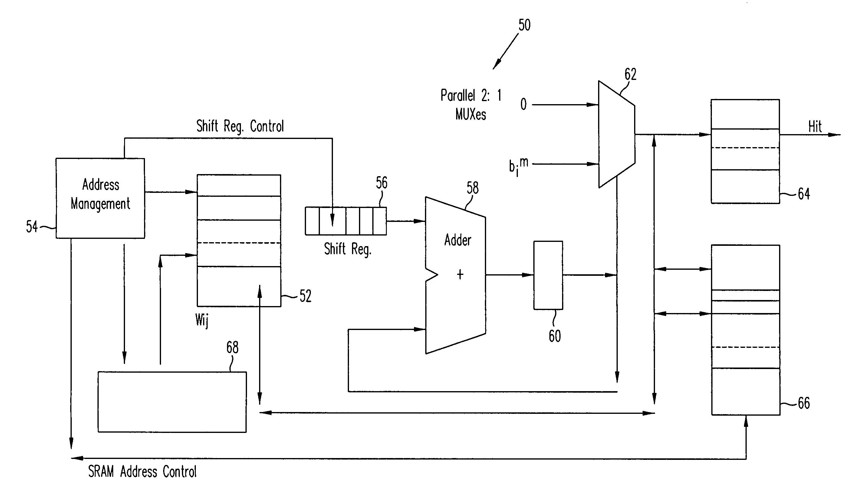
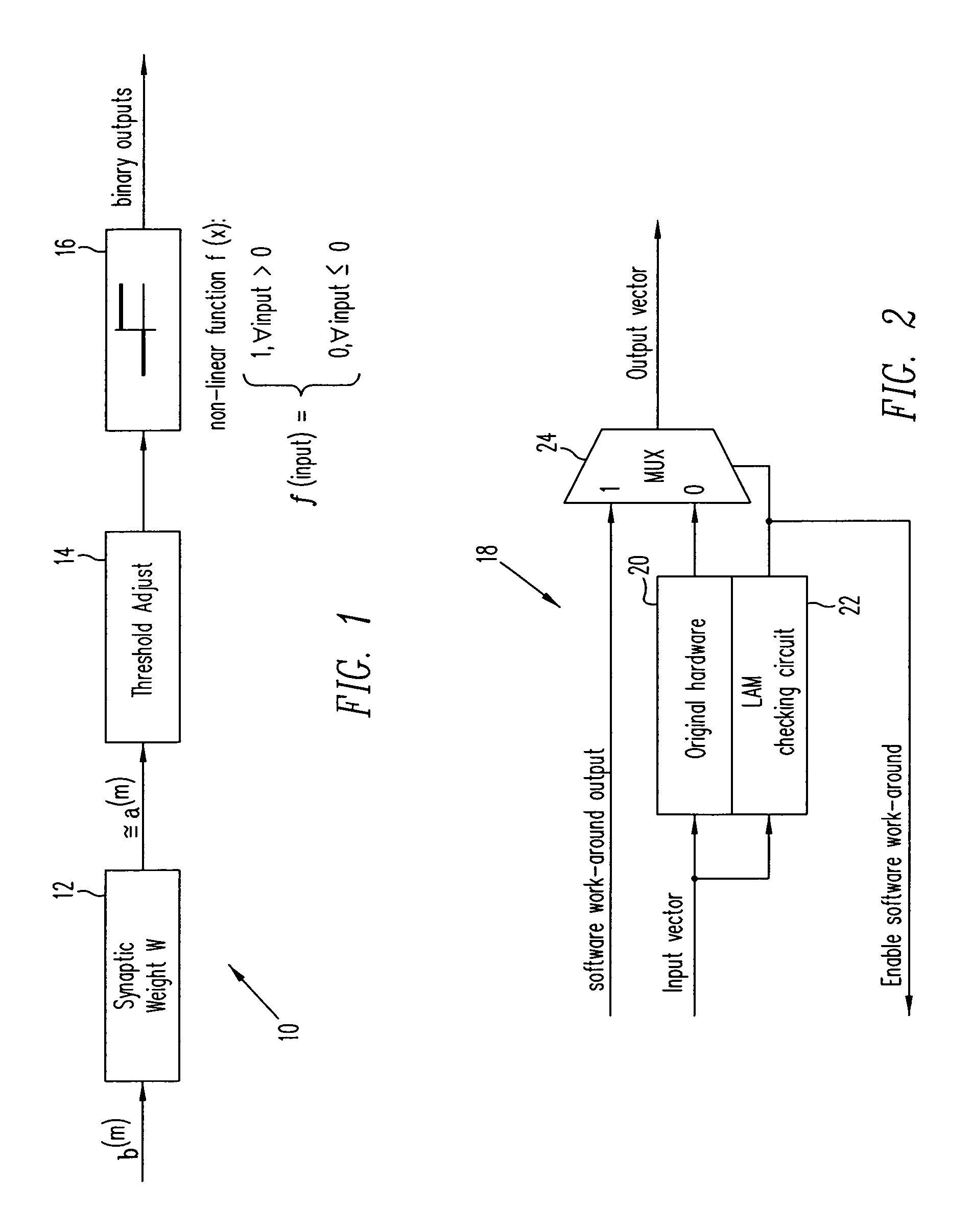
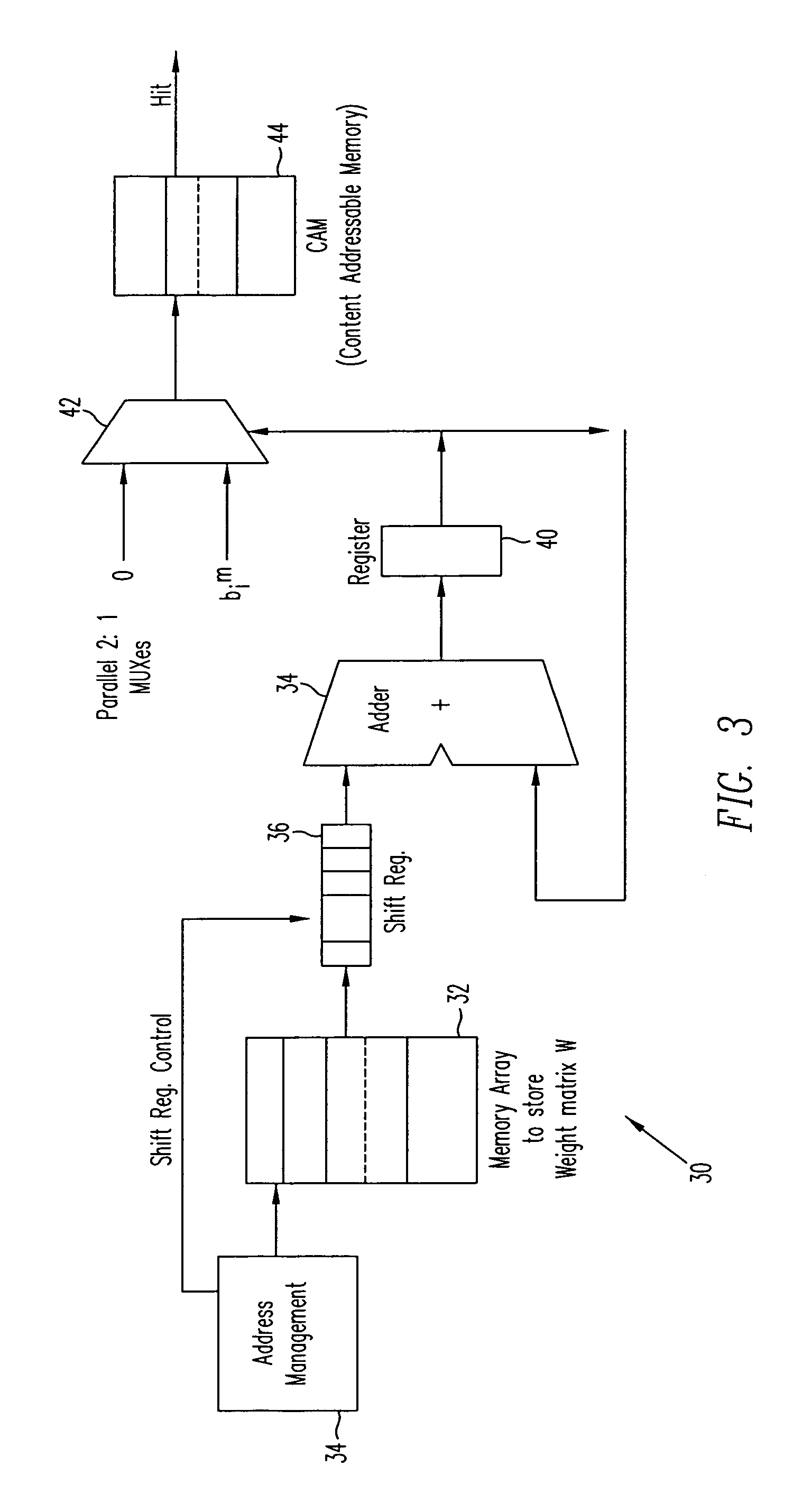
[0029]The present invention is directed to a method of providing fault-tolerance in a programmable logic circuit, such as an application-specific integrated circuit (ASIC) or field-programmable gate array (FPGA), by utilizing an efficient software work-around for faulty hardware in the programmable logic circuit. The hardware architecture envisioned by the invention allows for certain input vectors to be handled by the original hardware design while only faulty cases trigger the software work-around. In the preferred embodiment, this architecture is derived from a feedforward linear auto-associative memory neural network as discussed further below.

[0030]A generalized artificial neural network (ANN) with a feedforward linear associative memory (LAM) model has one layer of input neurons and one layer of output neurons, with a feedforward weight connection. A background discussion of this type of ANN can be found in the book “Digital Neural Networks,” by S. Y. Kung (1993). Feedforward...


PUM


Abstract

A programmable logic unit (e.g., an ASIC or FPGA) having a feedforward linear associative memory (LAM) neural network checking circuit which classifies input vectors to a faulty hardware block as either good or not good and, when a new input vector is classified as not good, blocks a corresponding output vector of the faulty hardware block, enables a software work-around for the new input vector, and accepts the software work-around input as the output vector of the programmable logic circuit. The feedforward LAM neural network checking circuit has a weight matrix whose elements are based on a set of known bad input vectors for said faulty hardware block. The feedforward LAM neural network checking circuit may update the weight matrix online using one or more additional bad input vectors. A discrete Hopfield algorithm is used to calculate the weight matrix W. The feedforward LAM neural network checking circuit calculates an output vector a(m) by multiplying the weight matrix W by the new input vector b(m), that is, a(m)=wb(m), adjusts elements of the output vector a(m) by respective thresholds, and processes the elements using a plurality of non-linear units to provide an output of 1 when a given adjusted element is positive, and provide an output of 0 when a given adjusted element is not positive. If a vector constructed of the outputs of these non-linear units matches with an entry in a content-addressable memory (CAM) storing the set of known bad vectors (a CAM hit), then the new input vector is classified as not good.

Description

BACKGROUND OF THE INVENTION[0001]1. Field of the Invention[0002]The present invention generally relates to electronic circuits, specifically, programmable logic units such as application-specific integrated circuits (ASICs) and field-programmable gate arrays (FPGAs), and more particularly to an improved method of overcoming design flaws in such programmable logic circuits, using software work-arounds in place of the defective portions of the circuits, but only for those input vectors affected by the fault.[0003]2. Description of the Related Art[0004]Modern electronic circuits use many different types of logic components or processing units to carry out numerous functions. In the early years of the semiconducting industry, these components were integrated circuits (ICs) with narrowly limited functionalities. Early small-scale integration ICs contained a few logic gates (AND gates, OR gates, NAND gates, NOR gates, XOR gates, etc.) amounting to a few dozen transistors. These gates are ...

Claims


Application Information

Patent Timeline
Patent Type & Authority Patents(United States)
IPC IPC(8): G06F12/00
CPCG01R31/318519G06N3/08G06N3/063
Inventor PHAM, CHRISTOPHER H.
Owner CISCO TECH INC
Why Eureka
Try Eureka