Semiconductor integrated circuit and a method of testing the same

a technology of integrated circuits and semiconductors, applied in the direction of individual semiconductor device testing, semiconductor/solid-state device testing/measurement, instruments, etc., can solve the problems of reducing the time required for testing, the inability to perform voltage trimming in parallel, and the process of lsis trimming one after another

Active Publication Date: 2006-02-14
RENESAS ELECTRONICS CORP
View PDF9 Cites 12 Cited by
  • Summary
  • Abstract
  • Description
  • Claims
  • Application Information

AI Technical Summary

Benefits of technology

[0006]In JP-A-5-265579, use of an on-chip comparator or a comparator on a tester as a comparator for comparison between the voltage obtained by trimming and the target voltage value is simply stated but no notice is taken of the difference between the two cases. In contrast, the inventors of the present invention took note of the following points. That is, trimming on a plurality of LSIs with one evaluation device is effective in reducing the time required for testing including a measuring operation for voltage trimming or the like, but this voltage trimming cannot be performed in a parallel manner because the external evaluation device measures the voltage. Only a limited effect may be obtained by performing voltage measurement and trimming register value adjustment while successively changing the objects by switching with a relay. The same can be said with respect to trimming for adjustment of the write pulse width and the erase pulse width determined by dividing a clock frequency generated from an internal oscillator, or the current through a MOS transistor determined by LSI manufacturing conditions. Thus, any process in which LSIs undergoes trimming one after another requires a considerably long test time.

Problems solved by technology

That is, trimming on a plurality of LSIs with one evaluation device is effective in reducing the time required for testing including a measuring operation for voltage trimming or the like, but this voltage trimming cannot be performed in a parallel manner because the external evaluation device measures the voltage.
Thus, any process in which LSIs undergoes trimming one after another requires a considerably long test time.

Method used


Image

  • Semiconductor integrated circuit and a method of testing the same
  • Semiconductor integrated circuit and a method of testing the same
  • Semiconductor integrated circuit and a method of testing the same

Examples


Embodiment Construction

>

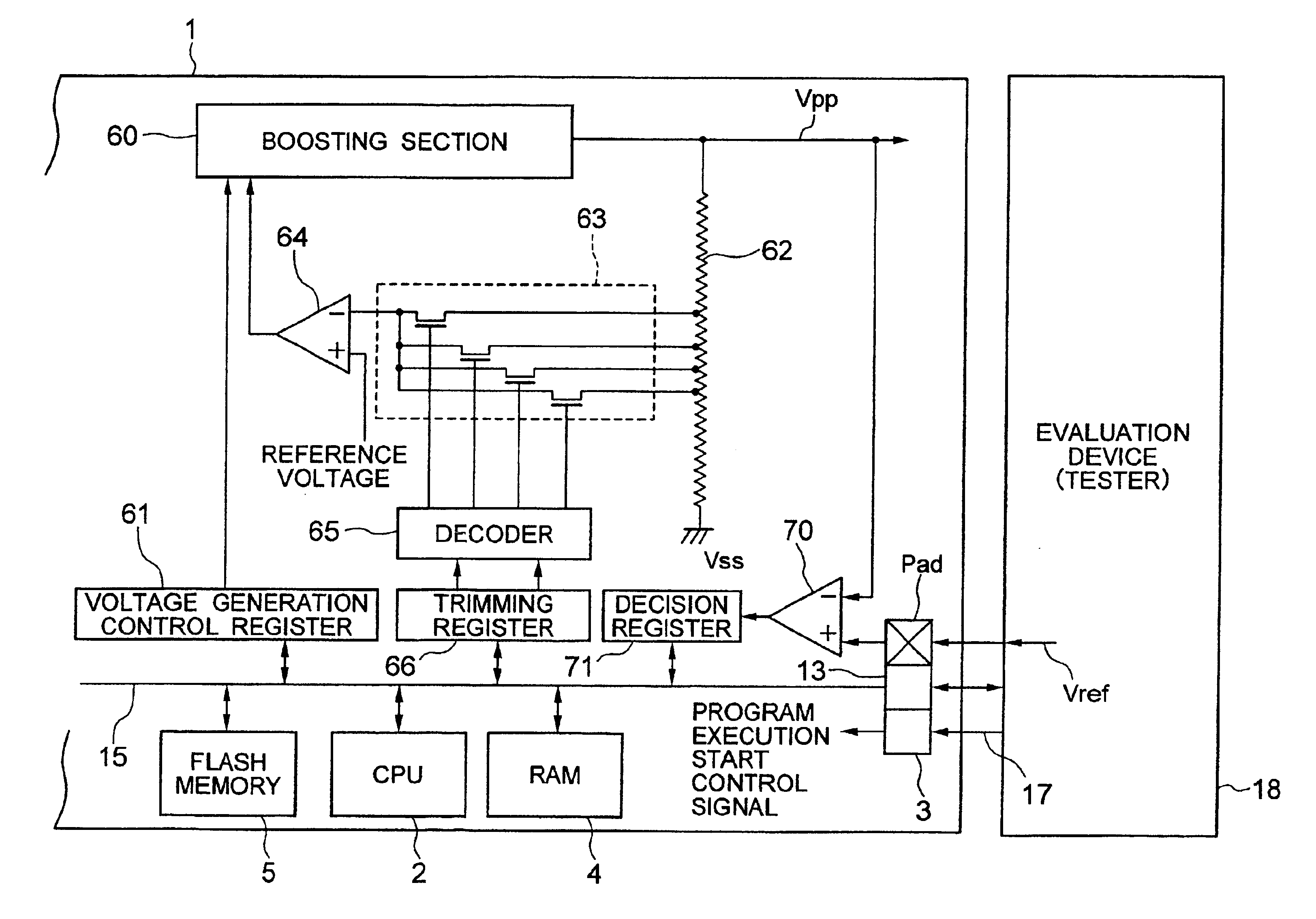
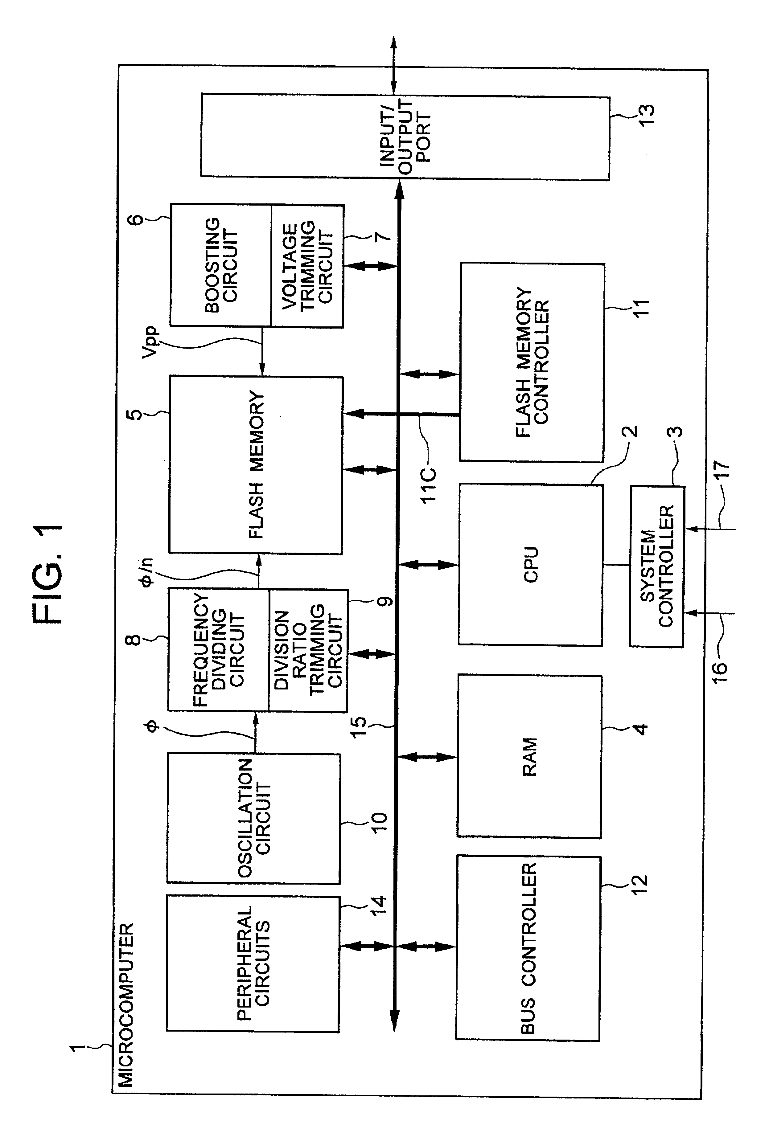
[0065]FIG. 1 illustrates a microcomputer 1 arranged as a data processor, which is an example of a semiconductor integrated circuit in accordance with the present invention. The microcomputer 1 shown in FIG. 1 is fabricated on one semiconductor substrate (semiconductor chip) such as a monocrystal silicon substrate by a well-known CMOS integrated circuit manufacturing technique, for example. As illustrated, the microcomputer 1 has a CPU 2 provided as a computation control circuit or a control circuit, a system controller 3, a RAM 4, which is a volatile memory, a flash memory 5, which is a nonvolatile memory, a boosting circuit 6, a voltage trimming circuit 7, a frequency divider circuit 8, a division ratio trimming circuit 9, an oscillator 10, a flash memory controller 11, a bus controller 12, an input / output port 13, and other peripheral circuits 14 including a timer. These circuit modules are connected to a bus 15, which includes an address bus, a data bus, and a control bus. The b...


PUM


Abstract

A semiconductor integrated circuit (LSI) in which control information for determining a voltage or a width of a pulse produced itself can easily be set in parallel with other LSIs, and set information can be corrected easily. From an external evaluation device, a voltage of an expected value is supplied in overlapping manner to a plurality of LSIs each having a CPU and a flash memory. Each LSI incorporates a comparison circuit comparing an expected voltage value and a boosted voltage generated in itself. The CPU refers to a comparison result and optimizes control data in a data register for changing a boosted voltage. The CPU controls the comparison circuit and the data register and performs trimming in a self-completion manner, thereby making, trimming on a plurality of LSIs easily in a parallel manner and a total test time reduced.

Description

BACKGROUND OF THE INVENTION[0001]The present invention relates to a trimming technique for finely adjusting a voltage, the width of a pulse, etc., produced in a semiconductor integrated circuit (large-scale integrated circuit (LSI)) in accordance with characteristics of LSI, and relates to a semiconductor integrated circuit such as a microcomputer incorporating a flash memory and to a testing method of performing trimming on such a semiconductor integrated circuit.[0002]There are some nonvolatile memories such as flash memories generating a particular programming voltage in LSIs. This voltage varies because of manufacturing variation and there is a need to perform trimming or fine adjustment for correcting the programming voltage in each LSI. The memory programming time characteristic also varies. Therefore, the programming voltage is changed according to the memory characteristics to constantly maintain memory programming characteristics.[0003]In fine adjustment (hereinafter referr...

Claims


Application Information

Patent Timeline
Patent Type & Authority Patents(United States)
IPC IPC(8): G01R31/28G01R31/30G01R31/317G06F15/78G11C16/02G11C17/00G11C29/02G11C29/12H01L21/66H01L21/822H01L27/04
CPCG01R31/30G01R31/31703G01R31/31725G01R31/3187G06F11/24G11C29/02G11C29/021G11C29/028G11C29/50012G11C2029/5004G11C16/04
Inventor TANAKA, TOSHIHIROSHINAGAWA, YUTAKAKIMURA, MASAHIKONAKAMURA, ISAO
Owner RENESAS ELECTRONICS CORP
Why Eureka
Try Eureka