Flash cell fuse circuit

a fuse circuit and flash memory technology, applied in the field of flash memory fuse circuits, can solve the problems of fuse circuits, invariably different operating characteristics of memory devices fabricated, wireless applications consuming large quantities of flash memory, etc., and achieve the effect of reducing manufacturing costs and improving the efficiency of die area

Inactive Publication Date: 2006-02-21
MICRON TECH INC
View PDF13 Cites 21 Cited by
  • Summary
  • Abstract
  • Description
  • Claims
  • Application Information

AI Technical Summary

Benefits of technology

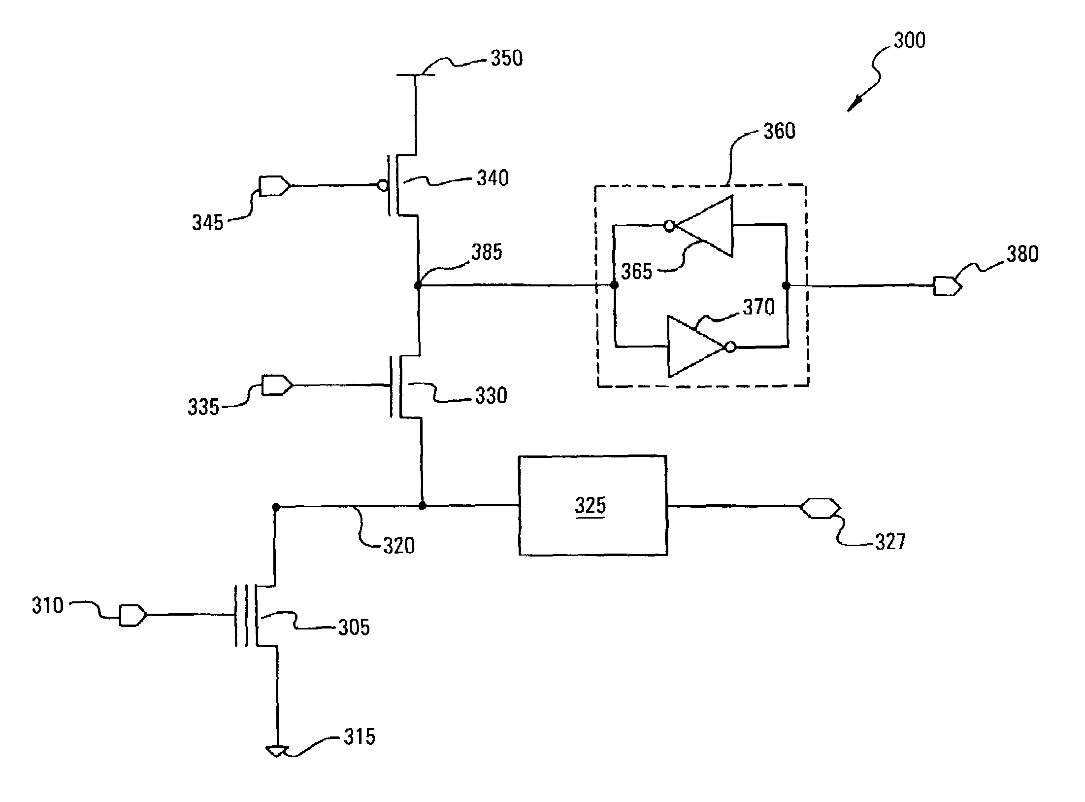
[0013]Fuse circuits based on a single flash cell or floating-gate memory cell are adapted for use in memory devices, particularly in low-voltage applications. Such fuse circuits include a floating-gate memory cell for storing a data value and a fuse latch to hold and transfer the data value of the floating-gate memory cell at power-up or upon request. A latch driver circuit can write data values to the fuse latch without affecting the data value stored in the floating-gate memory cell. The ability to write to the fuse latch without affecting the stored data value can be useful in testing of the memory device. The fuse circuits can further utilize the same structure, pitch, bit-line organization and word-line organization as the memory device's memory array, thus simplifying fabrication and leading to more efficient use of die area. As the fuse circuits can utilize the same structure and organization, the data value of the fuse circuit can be programmed, erased and read using the same data path as the regular memory array.

Problems solved by technology

Digital cellular and wireless applications consume large quantities of flash memory and are continually pushing for lower operating voltages and higher densities.
Although attempts have been made to carefully control the fabrication of such memory devices so as to increase their yield, there invariably will be differences in operating characteristics of memory devices fabricated at different times. These differences in operating characteristics are primarily due to processing variations and may even occur between different semiconductor wafers in a single batch of wafers.
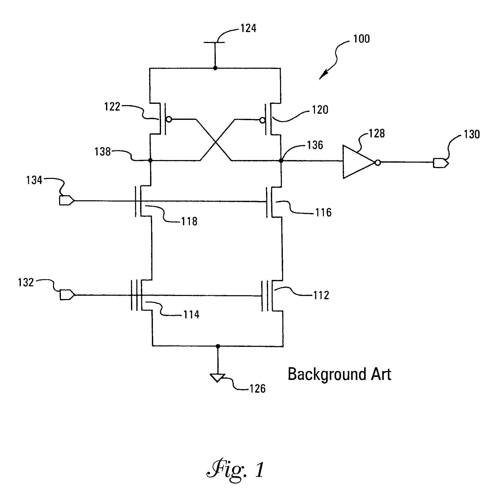
As device operating voltages are reduced, fuse circuits of the type shown in FIG. 1 may become inoperable or may latch too slowly for effective operation.

Method used


Image

  • Flash cell fuse circuit
  • Flash cell fuse circuit
  • Flash cell fuse circuit

Examples


Embodiment Construction

[0024]In the following detailed description of the present embodiments, reference is made to the accompanying drawings that form a part hereof, and in which is shown by way of illustration specific embodiments in which the invention may be practiced. These embodiments are described in sufficient detail to enable those skilled in the art to practice the invention, and it is to be understood that other embodiments may be utilized and that process, electrical or mechanical changes may be made without departing from the scope of the present invention. The terms wafer or substrate used in the following description include any base semiconductor structure. Examples include silicon-on-sapphire (SOS) technology, silicon-on-insulator (SOI) technology, thin film transistor (TFT) technology, doped and undoped semiconductors, epitaxial layers of a silicon supported by a base semiconductor structure, as well as other semiconductor structures well known to one skilled in the art. Furthermore, whe...


PUM


Abstract

Fuse circuits based on a single flash cell or floating-gate memory cell are adapted for use in memory devices, particularly in low-voltage, flash memory applications. The fuse circuits include a floating-gate memory cell for storing a data value and a fuse latch to hold and transfer the data value of the floating-gate memory cell at power-up or upon request. A latch driver circuit can write data values to the fuse latch without affecting the data value stored in the floating-gate memory cell. The fuse circuits can further utilize the same structure, pitch, bit-line organization and word-line organization as the memory device's memory array. As the fuse circuits can utilize the same structure and organization, the data value of the fuse circuit can be programmed, erased and read using the same data path as the regular memory array.

Description

[0001]This application is a divisional of U.S. patent application Ser. No. 09 / 943,643 (allowed), filed Aug. 30, 2001 U.S. Pat. No. 6,654,272 and titled, “FLASH CELL FUSE CIRCUIT” which is commonly assigned and incorporated by reference in its entirety herein, and which claims priority to Italian Patent Application Serial No. RM2001A000105 filed Feb. 27, 2001, which is commonly assigned. The present invention relates generally to semiconductor memory devices, and in particular, the present invention relates to flash cell (floating-gate memory cell) fuse circuits, their applications and their operation.TECHNICAL FIELD OF THE INVENTIONBackground of the Invention[0002]Electronic information handling or computer systems, whether large machines, microcomputers or small and simple digital processing devices, require memory for storing data and program instructions. Various memory systems have been developed over the years to address the evolving needs of information handling systems. One s...

Claims


Application Information

Patent Timeline
Patent Type & Authority Patents(United States)
IPC IPC(8): G11C17/00G11C16/20G11C16/26G11C17/18G11C29/00
CPCG11C16/0441G11C16/20G11C29/789G11C17/18G11C16/26
Inventor SANTIN, GIOVANNINASO, GIOVANNI
Owner MICRON TECH INC
Why Eureka
Try Eureka