Process for automated generation of design-specific complex functional blocks to improve quality of synthesized digital integrated circuits in CMOS using altering process

a technology of complex functional blocks and process, applied in the field of automatic system and process for creating highly optimized transistorlevel building blocks, can solve the problems of large cost and business implications, poor final design quality, and relatively poor resultant design quality

Inactive Publication Date: 2006-02-21
OPEN-SILICON
View PDF7 Cites 38 Cited by
  • Summary
  • Abstract
  • Description
  • Claims
  • Application Information

AI Technical Summary

Benefits of technology

[0014]In light of the shortcomings of automated IC design processes discussed above, the present invention focuses on the automated creation of functional IC design building blocks (i.e., cells) using a plurality of transistor level optimization techniques. Consequently, the present invention enriches the original library with new cells that are particularly suitable for specific IC designs. The present invention can take into account a plurality of constraints that may apply to cells in the implementation of the IC design. The design-specific cells designed in accordance with the present teachings tend to be larger than standard IC design cells made of pre-defined (i.e., standard) cells. The size of the present invention's cells can be optimized by IC design criteria so that (i) performance of the resultant cells is within acceptable limits, and (ii) the generated cells can be interfaced using existing automated layout synthesis tools. While the present invention is primarily focused on generation of cells in the CMOS designs, it should be appreciated by those skilled in the art that this invention can also used for creating cells for use in other types of IC designs, including various forms of “dynamic CMOS” and / or a combination of static CMOS and dynamic CMOS.

Problems solved by technology

Place-and-route tools also take into account the detailed timing issues that arise from the actual location of the various cells in the layout.
A key problem with the existing approach of automated IC design processes is that designers, using synthesis tools, are forced to use components from a static, pre-defined standard-cell library of cells developed to be applicable to a wide variety of digital ICs.
However, for a given design, the forced use of such pre-defined standard cells leads to poor quality in the final design as compared to full-custom (hand-crafted) IC design processes and judged by the aforementioned quality metrics.
Therefore, although automated tools and flows speed up the design creation process, the relatively poor quality of resultant designs as judged against the quality that can be achieved with a manual re-design of the same part, has major cost and business implications.
Recently, it has been noted by many designers and researchers that this profusion of metal interconnects in automatically generated designs constitutes an increasing problem (and bottleneck) in terms of performance and power consumption, as IC designs into deep-sub-micron geometries approaching 0.10 micron or less.
The vast majority of industrial standard-cell based designs continue to use static CMOS style of design, due to various problems inherent in PTL.
Key among such problems is the loss of one V_t (threshold voltage of a transistor, modified by appropriate body effects) while passing a signal (high or low voltage) through pass transistors, which can easily lead to slow / improper functioning of subsequent stages of transistors driven by a pass transistor.
The prior automated IC design processes do not take into account performance of the resultant modules as well as a host of real-life constraints that must be taken into account while creating transistor-level modules used in actual designs.

Method used


Image

  • Process for automated generation of design-specific complex functional blocks to improve quality of synthesized digital integrated circuits in CMOS using altering process
  • Process for automated generation of design-specific complex functional blocks to improve quality of synthesized digital integrated circuits in CMOS using altering process
  • Process for automated generation of design-specific complex functional blocks to improve quality of synthesized digital integrated circuits in CMOS using altering process

Examples


Embodiment Construction

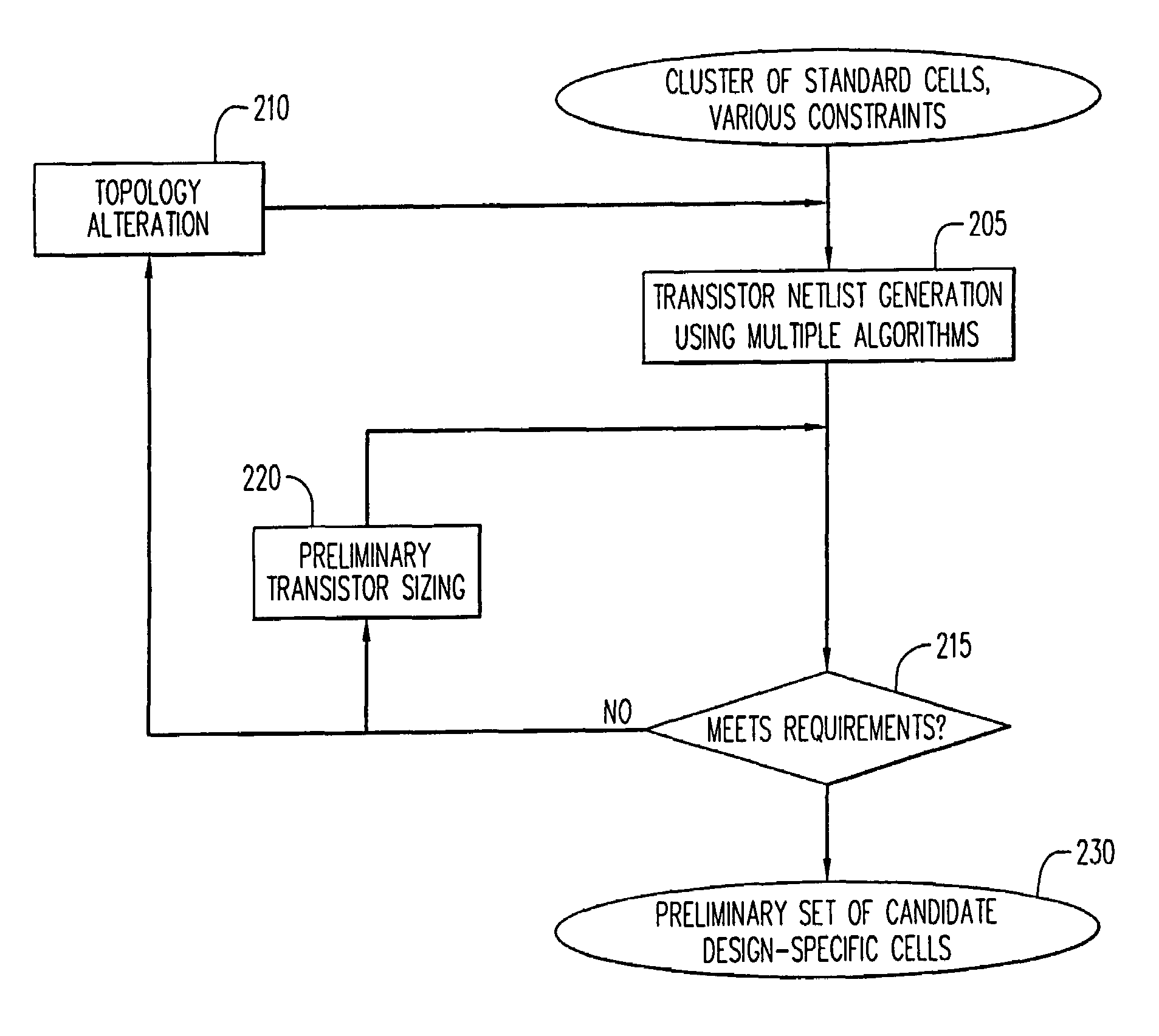
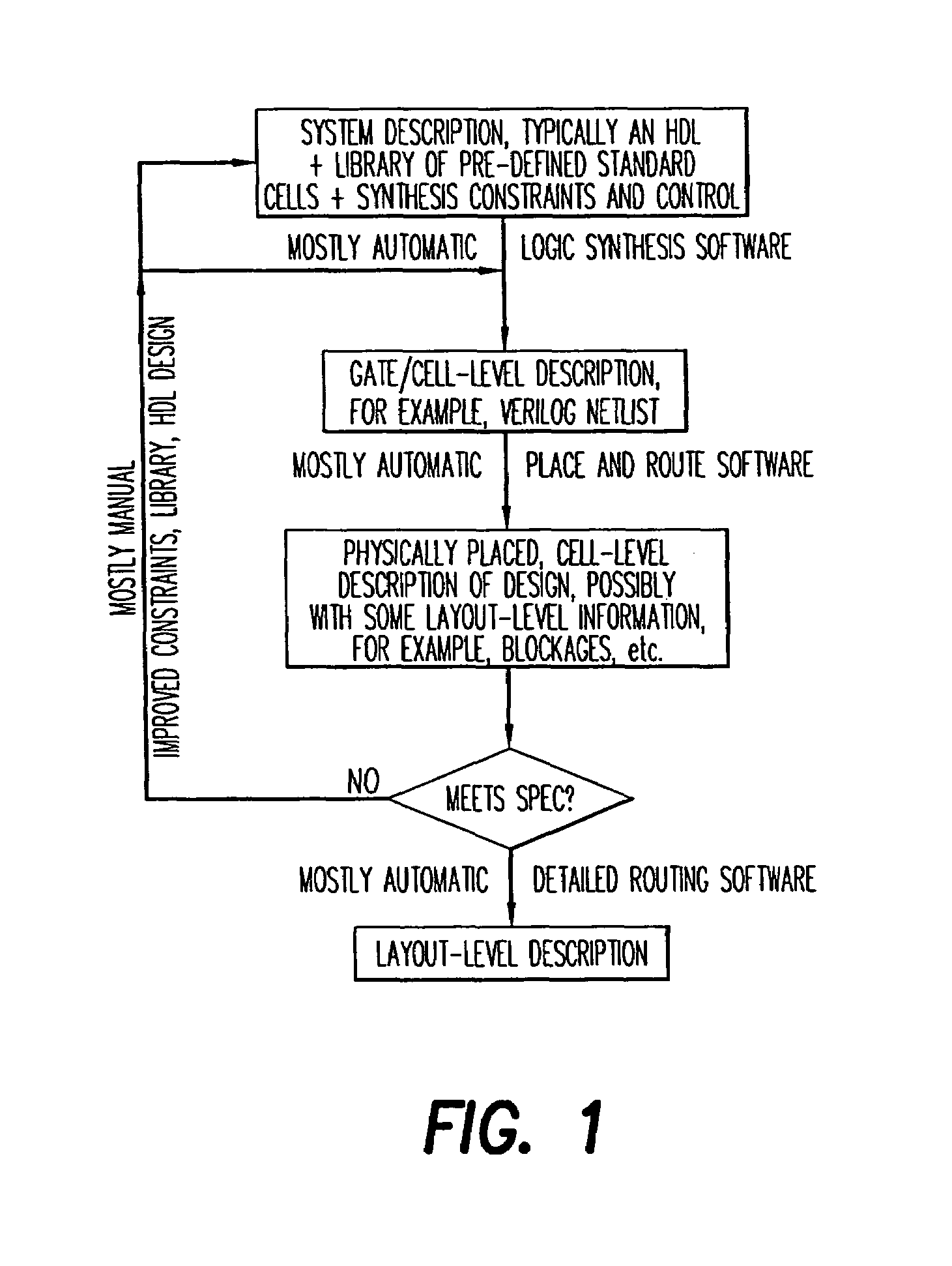
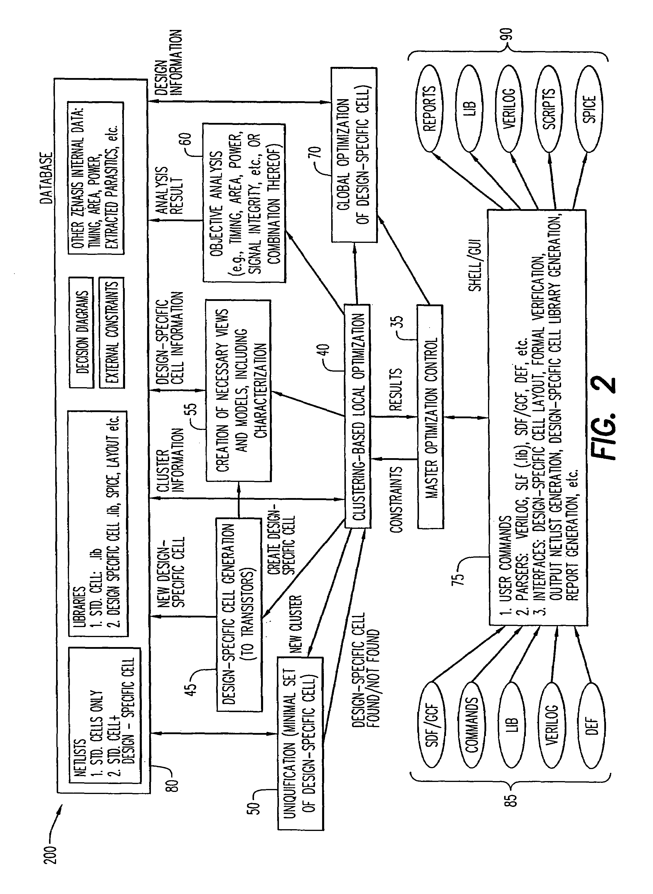
[0023]The present invention is a fully automated process capable of creation and optimization of design-specific, complex functional blocks, hereinafter designated design-specific cells. The use of design-specific cells in an automated IC design process has a very significant impact on the quality of the resultant design. The process of the present invention, in one aspect thereof, bridges the gap between designs created automatically and handcrafted designs. A fuller understanding of the overall organization of an IC design process using design-specific cells created in accordance with the present invention for designing high-quality, design-specific ICs can be had by referring to FIG. 2. The process of generating the design-specific IC design building blocks is represented as design-specific cell generation process 45.

[0024]In clustering process 40, prior to the invocation of the creation of the design-specific cell(s), the functionality of each target design-specific cell is iden...


PUM


Abstract

The present invention pertains to an automated method for designing a integrated circuit (IC) design-specific cell, the method includes the steps of receiving a design specification for the design-specific cell, mapping a transistor-level representation of the design-specific cell, wherein the mapping is based on at least one, but perhaps plural design specifications, and evaluating the transistor-level representation of the design-specific cell for satisfaction of the design specification.

Description

[0001]This application is related to U.S. Provisional Patent Application No. 60 / 215,523, filed on Jun. 30, 2000.BACKGROUND OF THE INVENTION[0002]1. Field of the Invention[0003]This invention relates to the design of integrated circuits (ICs) in general, and in particular to an automated system and process for creating highly optimized transistor-level building blocks that incorporate design-specific optimization goals and yields significant benefits for most design environments, such as, COT / COL, ASICS, ASP, etc.[0004]2. Description of the Related Art[0005]Over the last four decades, design and manufacturing of ICs has evolved into a multi-billion dollar industry. IC designs can be broadly classified into two major categories: (i) storage designs, which store digital data; and (ii) logic designs, which manipulate digital data.[0006]The present invention described herein is applicable to the category of logic ICs or parts thereof, that deal broadly with data manipulation and several ...

Claims


Application Information

Patent Timeline
Patent Type & Authority Patents(United States)
IPC IPC(8): G06F17/50
CPCG06F17/5068G06F17/505G06F30/327G06F30/39
Inventor BHATTACHARYA, DEBASHISBOPPANA, VAMSIMURGAI, RAJEEVROY, RABINDRA
Owner OPEN-SILICON
Why Eureka
Try Eureka