Semiconductor device and method of manufacturing the same

Inactive Publication Date: 2006-03-07
RENESAS TECH CORP
View PDF5 Cites 5 Cited by
  • Summary
  • Abstract
  • Description
  • Claims
  • Application Information

AI Technical Summary

Benefits of technology

[0008]Accordingly, an object of the invention is to provide a structure and a manufacturing method of a semiconductor device, which is provided with a bipolar transistor and an MOS transistor, can lower a saturation voltage of the MOS transistor without lowering a breakdown voltage between elements of the bipolar transistor.

Problems solved by technology

However, the low concentration in the second epitaxial layer impairs a breakdown voltage between a collector and a base of the npn transistor.

Method used


Image

  • Semiconductor device and method of manufacturing the same
  • Semiconductor device and method of manufacturing the same
  • Semiconductor device and method of manufacturing the same

Examples


first embodiment

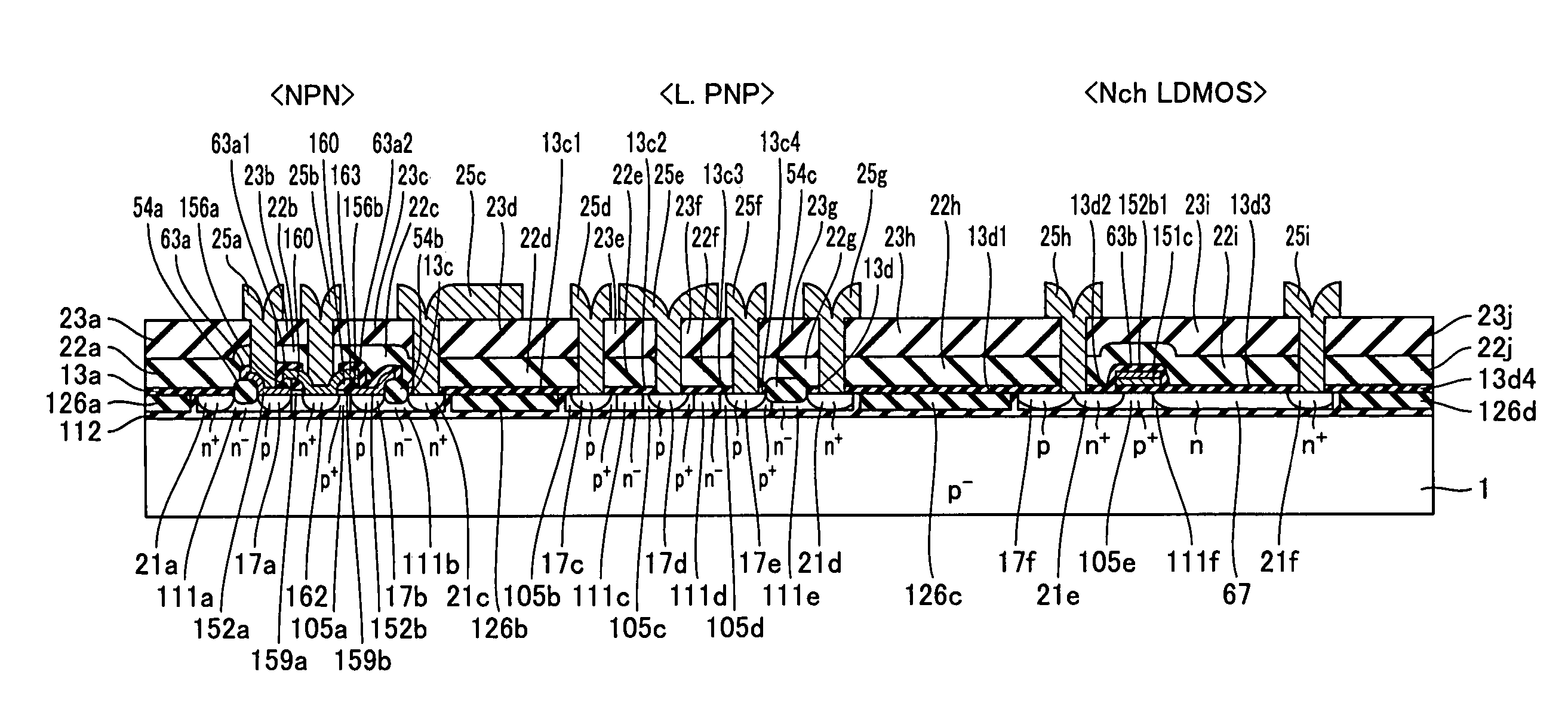
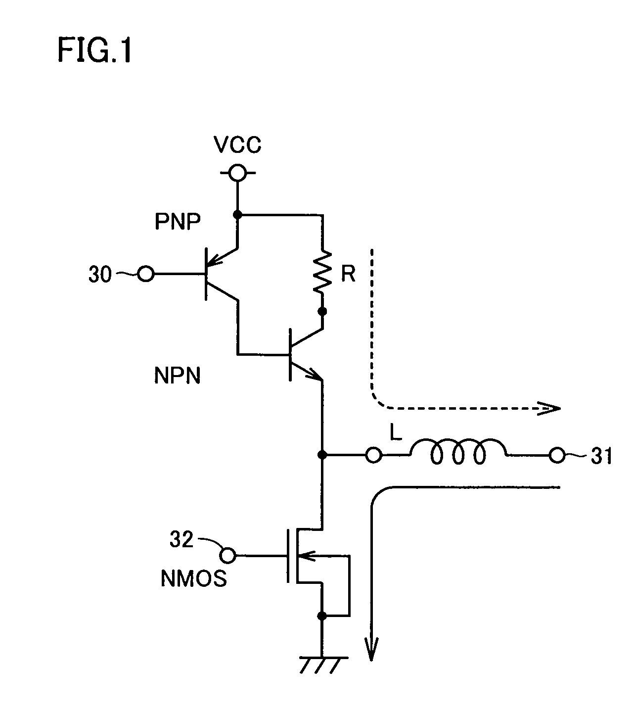
[0039](First Embodiment)

[0040]FIG. 1 is an equivalent circuit diagram of a semiconductor device (semiconductor integrated circuit) according to a first embodiment. As shown in FIG. 1, bipolar transistors are used in an output circuit of the semiconductor device.

[0041]It is assumed that a large equivalent inductor L is present on an output destination. An output transistor on a power supply Vcc side (upper side in FIG. 1) is formed of a Darlington connection of pnp and npn transistors. More specifically, an emitter of the pnp transistor is connected to a power supply terminal, a collector of the npn transistor is connected to the power supply terminal via a resistance (R), and a collector of the pnp transistor is connected to a base of the npn transistor. A collector current of the pnp transistor directly drives the base of the npn transistor. The Darlington connection thus formed provides the transistors effectively having a high current amplification factor hFE. By providing resist...

second embodiment

[0101](Second Embodiment)

[0102]A second embodiment of the invention will now be described with reference to FIGS. 34 to 37.

[0103]In the first embodiment described above, contact resistances may rise due to miniaturization of the elements. Accordingly, a device, which can suppress rising of the contact resistance, will now be described as a second embodiment.

[0104]FIG. 37 shows an example of a distinctive structure of the semiconductor device according to the second embodiment. As shown in FIG. 37, p+-diffusion layers (heavily doped impurity diffusion layers) 71a, 71b, 71c and 71d are formed at the surface of p-type diffusion layers 17a, 17c, 17d and 17e, respectively. p+-diffusion layers 71a–71d contain p-type impurities at higher concentrations than p-type diffusion layers 17a, 17c, 17d and 17e, respectively. The concentrations of p-type impurities contained in p+-diffusion layers 71a–71d are substantially in a range from about 1×1019 cm−3 to about 1×1021 cm−3.

[0105]Silicide layers...

third embodiment

[0116](Third Embodiment)

[0117]A third embodiment of the invention will now be described with reference to FIGS. 38–51.

[0118]A Hetero-junction Bipolar Transistor (HBT) of an SiGe base is a high-frequency bipolar transistor for use in the next generation of the ultra-high speed communication system (optical communication system of 10 Gb / s or higher, wireless LAN, mobile communication system and others).

[0119]For producing a high-frequency npn transistor, it is necessary to reduce a thickness of the base. However, if the thickness of the base is reduced, it is difficult to ensure a collector-emitter breakdown voltage. Conversely, the collector-emitter breakdown voltage can be ensured by increasing the concentration of impurities in the base. However, this impedes ensuring of an intended base-emitter breakdown voltage.

[0120]In view of the above, the base of the npn transistor may be made of an epitaxial growth layer (e.g., containing 10%–30% of Ge) of SiGe providing a narrower band gap ...


PUM


Abstract

A semiconductor device includes a p−-silicon substrate, n−-epitaxial growth layers on the p−-silicon substrate, a field insulating film at the surface of the n−-epitaxial growth layer, an npn transistor formed at the n−-epitaxial growth layer, an pnp transistor formed at the n−-epitaxial growth layer, a DMOS transistor on the n−-epitaxial growth layer, and a resistance. The DMOS transistor includes an n+-diffusion layer forming a source, a p-type diffusion layer forming a back gate region, a lightly doped n-type diffusion layer forming a drain, and a heavily doped n+-diffusion layer forming the drain.

Description

BACKGROUND OF THE INVENTION[0001]1. Field of the Invention[0002]The invention relates to a semiconductor device and a method of manufacturing the same, and particularly to a semiconductor device provided with a DMOS (Double-Diffused Metal Oxide Semiconductor) and a bipolar transistor as well as a method of manufacturing the same.[0003]2. Description of the Background Art[0004]A semiconductor device employing a bipolar transistor in an output circuit has been known. For example, Japanese Patent Laying-Open No. 5-3293 has disclosed a semiconductor integrated circuit for providing an output-stage inverter circuit formed of a combination of a vertical PNP transistor and a DMOSFET.[0005]As related arts, Japanese Patent Laying-Open No. 8-227945 has disclosed a method of forming an integrated circuit based on a BiCDMOS process, and Japanese Patent Laying-Open No. 2002-198448 has disclosed a method of manufacturing a semiconductor device by a BiCMOS process.[0006]In the semiconductor integr...

Claims


Application Information

Patent Timeline
IPC IPC(8): H01L31/119H01L21/28H01L21/336H01L21/8249H01L27/04H01L27/06H01L27/12H01L29/06H01L29/08H01L29/10H01L29/73H01L29/732H01L29/735H01L29/78H01L29/786
CPCH01L21/8249H01L27/0623H01L29/7816H01L29/66674H01L29/7317H01L29/7322H01L29/735H01L29/0696H01L29/0847H01L29/1083H01L29/66681H01L29/7824A61H23/006A61H39/04A61H2201/1253A61H2205/021A61H2201/1695
Inventor NAKASHIMA, TAKASHI
Owner RENESAS TECH CORP
Why Eureka
Try Eureka