

Method for preventing formation of photoresist scum
a photoresist and scum technology, applied in the field of semiconductor process, can solve the problems of difficult removal, device failure, and serious affecting the electrical properties of the device, and achieve the effect of preventing the formation of photoresist scum and preventing nitrogen from contaminating the photoresis
- Summary
- Abstract
- Description
- Claims
- Application Information
AI Technical Summary
Benefits of technology
Problems solved by technology
Method used
Image

Examples
first embodiment
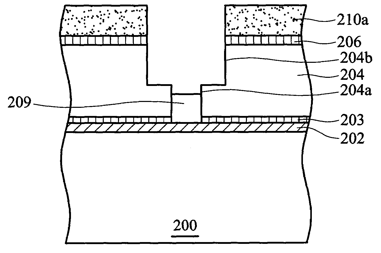
[0021]FIGS. 2a to 2e are cross-sections illustrating the method flow of preventing formation of photoresist scum according to the present invention.
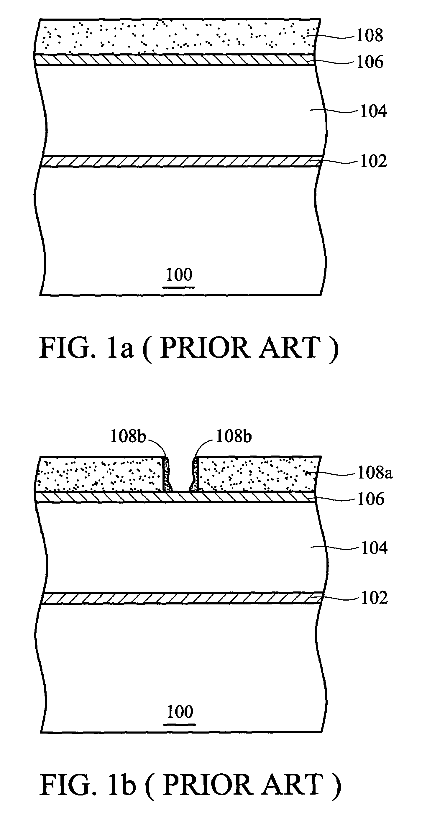
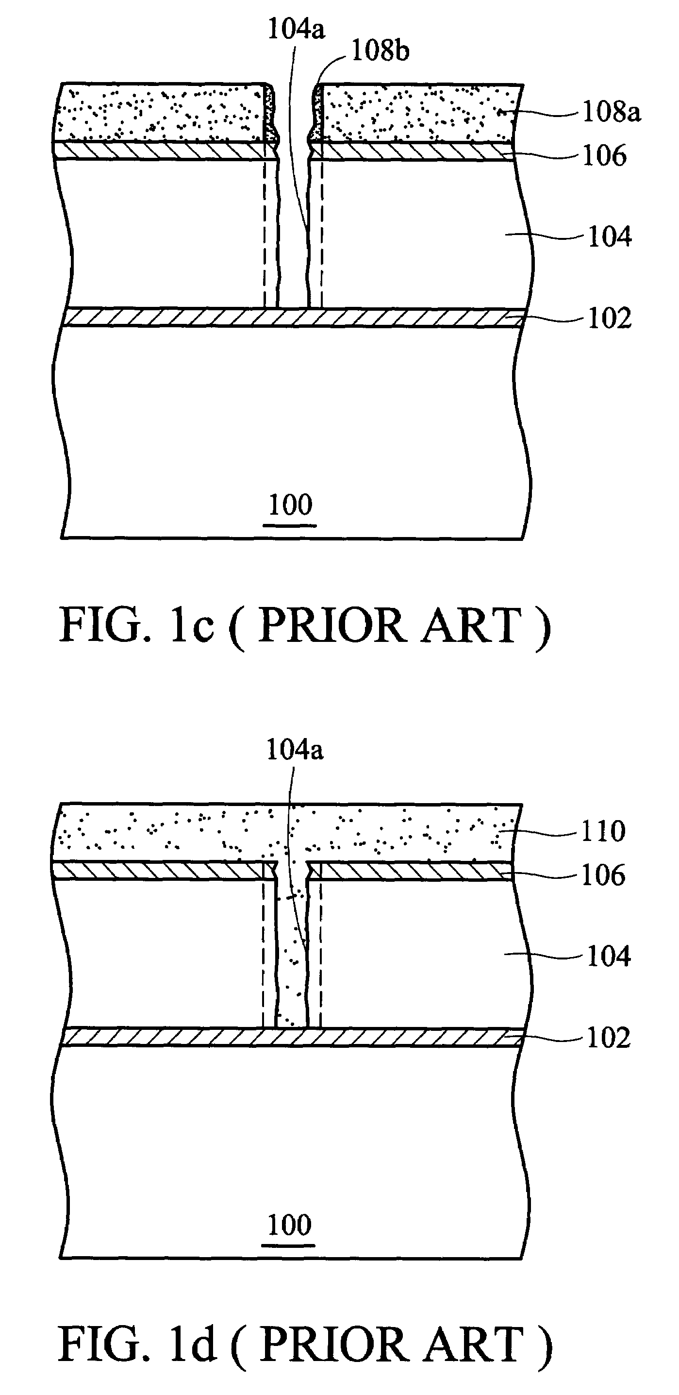
[0022]First, in FIG. 2a, a substrate 200 such as a silicon wafer is provided. Although there are semiconductor devices formed on the substrate 200, a flat substrate is depicted for simplicity. Next, an etching stop layer 202, a barrier layer 203, and a dielectric layer 204 are successively formed on the substrate 200. The material of the etching stop layer 202 can constitute silicon nitride or silicon carbon nitride. The barrier layer 203 can comprise silicon-rich oxide (SiOx) or hydrocarbon-containing silicon-rich oxide (SiOxCy:H), where x202 from diffusing into the dielectric layer 204. In addition, in the present embodiment, the etching stop layer 202 can also use material containing no nitrogen, such as silicon-rich oxide (SiOx) or hydrocarbon-containing silicon-rich oxide (SiOxCy:H) where x203. Next, a non-nitrogen anti-reflective l...
second embodiment
[0027]FIGS. 3a to 3e are cross-sections illustrating the method flow of preventing formation of photoresist scum according to the present invention.
[0028]First, in FIG. 3a, a substrate 300, such as a silicon wafer is provided. Next, an etching stop layer 302, a barrier layer 303, a dielectric layer 304, a barrier layer 305, an anti-reflective layer 306, and a photoresist layer 308 are formed on the substrate 300 in sequence. The etching stop layer 302 can comprise silicon nitride or silicon carbon nitride. The anti-reflective layer 306 can be silicon oxynitride. The barrier layers 305 and 303 can comprise silicon-rich oxide (SiOx) or hydrocarbon-containing silicon-rich oxide (SiOxCy:H), where x302 and in the anti-reflective layer 306 from diffusing into the dielectric layer 304.
[0029]Subsequently, in FIG. 3b, a photoresist pattern layer 308a is formed using conventional exposure and wet development procedures. Next, in FIG. 3c, the anti-reflective layer 306, the barrier layer 305, t...
PUM
| Property | Measurement | Unit |
|---|---|---|
| dielectric | aaaaa | aaaaa |
| thickness | aaaaa | aaaaa |
| electrical properties | aaaaa | aaaaa |
Abstract
Description
Claims
Application Information