Analog to digital converter circuit of successive approximation type operating at low voltage

a converter circuit and analog to digital converter technology, applied in the field of analog to digital converter circuits, can solve the problems of increasing leak current, difficult to realize ad converter circuits or digital to analog converters, and inability to use cmos analog switches as configured by p channel mosfets and n channel mosfets, etc., and achieve the effect of simple circuit configuration

Inactive Publication Date: 2006-03-21
SEMICON TECH ACADEMIC RES CENT
View PDF5 Cites 72 Cited by
  • Summary
  • Abstract
  • Description
  • Claims
  • Application Information

AI Technical Summary

Benefits of technology

[0042]Accordingly, the analog to digital converter circuit according to the present invention can realize the switched amplifier by the grounded switches operating at the low voltage, namely, by a rail to rail amplifier operable at input and output voltages in a range from the ground potential to the power supply voltage. Further, by outputting the output voltage from the hold capacitor of the sample hold circuit as the output voltage from the digital to analog converter via a common terminal thereto, and comparing the output voltage from the digital to analog converter with the appropriately set third potential using the comparator, the analog to digital converter circuit according to the present invention can perform a successive approximation operation and the digital to analog conversion. Since it suffices that the comparator detects only the difference between the reference voltage having the third potential and the output voltage from the digital to analog converter, the comparator can be configured by a simple circuit configuration. In addition, since the analog to digital converter circuit does not depend on a direct-current voltage of the input analog signal, the input voltage range of the analog to digital converter circuit can be set to the range from the ground potential to the voltage of the power supply voltage source. In the other words, the analog to digital converter circuit according to the present invention can operate at the power supply voltage equal to or lower than 1 V, and enlarges the input analog signal voltage range to the range from the ground potential to the voltage of the power supply voltage source. In addition, the analog to digital converter circuit can realize the comparator by the comparator having the narrow common-mode input voltage range, and execute a high-accuracy conversion without any influence of the offset voltage of the comparator and any influence of the parasitic capacitor of the capacitor array.

Problems solved by technology

However, as the Vth / Vdd ratio increases, an ordinary CMOS analog switch as configured by a P channel MOSFET and an N channel MOSFET cannot be used.
In such conditions, there is caused such a problem that it is difficult to realize an AD converter circuit or a digital to analog converter (referred to as a DA converter hereinafter) using an analog switch.
In order to solve the above-mentioned problem, when the threshold voltage Vth of the MOSFET is lowered, the ON resistance thereof decreases but an OFF resistance is not sufficiently high so that a leak current increases.
This leads to that the analog switch cannot be used.
However, these methods requires a device having a withstand voltage higher than that of an ordinary device, and this leads to such problems as complication of the process, deterioration of the reliability, and increase in the circuit area.
However, this leads to such problems as complication of the circuit configuration, decrease in the operation rate, and increase in the power consumption.

Method used


Image

  • Analog to digital converter circuit of successive approximation type operating at low voltage
  • Analog to digital converter circuit of successive approximation type operating at low voltage
  • Analog to digital converter circuit of successive approximation type operating at low voltage

Examples


first preferred embodiment

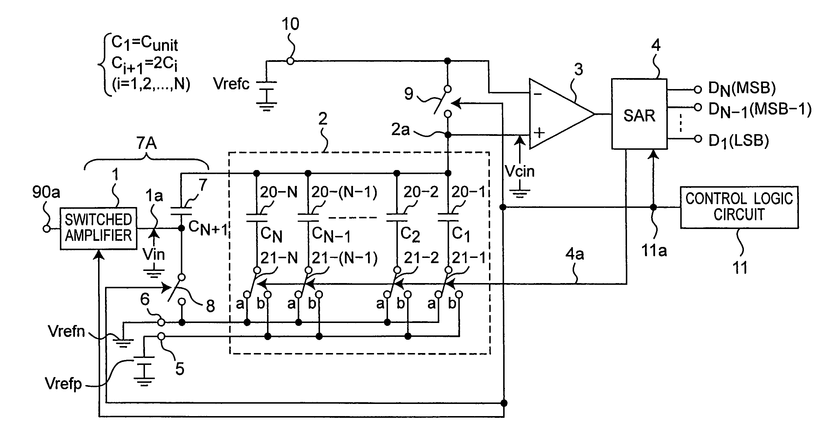
[0071]FIG. 1 is a circuit diagram showing a configuration of an AD converter circuit according to a first preferred embodiment of the present invention. The AD converter circuit according to the first preferred embodiment is an AD converter of successive approximation type that includes a local DA converter 2 using grounded switches each having one end connected to a ground potential (or a potential near the ground potential) Vrefn or a reference voltage source Vrefp, a sample hold circuit 7A as configured by a switched amplifier 1 and a hold capacitor 7, and a comparator 3 as configured to be simpler to have a less wide common-mode input voltage range than that of the prior art examples. The AD converter circuit according to the first preferred embodiment is characterized by being able to operate at a power supply voltage Vdd equal to or lower than 1 V.

[0072]Referring to FIG. 1, the switched amplifier 1 samples an input analog signal inputted via an input analog signal terminal 90a...

second preferred embodiment

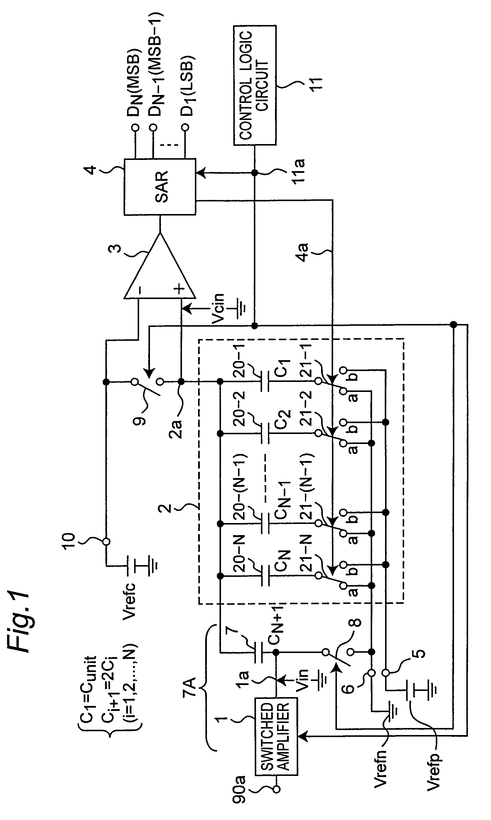
[0102]FIG. 15 is a circuit diagram showing a configuration of an AD converter circuit according to a second preferred embodiment of the present invention. The AD converter circuit according to the second preferred embodiment is characterized, as compared with that according to the first preferred embodiment, in that a voltage polarity of each of the capacitors 20-1 to 20-N is inverted, one end of the hold capacitor 7 is connected to the terminal 5 via the switch 8, and in that during sampling and holding, after lower one end of each of the capacitors 20-1 to 20-N is connected to the reference voltage source Vrefp, a successive approximation process of a control logic circuit 11A is performed as described below in detail by increasing voltages of sampled values, then successively reducing the voltages, and then making a comparison during successive approximation.

[0103]In an AD converter circuit of successive approximation type shown in FIG. 15, an input analog signal is sampled by a ...

third preferred embodiment

[0106]FIG. 16 is a circuit diagram showing a configuration of an AD converter circuit according to a third preferred embodiment of the present invention. The AD converter circuit according to the third preferred embodiment is characterized, as compared with that according to the first preferred embodiment shown in FIG. 1, by further including an additional capacitor 12 having a capacitance Cs between a connection line of an output voltage 2a from the DA converter 2 and the terminal 5. In the AD converter circuit according to the third preferred embodiment as configured as described above, the additional hold capacitor 12 can control the maximum amplitude of the output voltage Vcin from the DA converter 2. If the additional hold capacitor 12 is not provided (in case of FIG. 1), and the output voltage from the DA converter 2 is defined as a voltage Vcin and that the output voltage of the switched amplifier 1 is defined as a voltage Vin, then the output voltage Vin is represented by th...


PUM


Abstract

In a sampling and holding, a control logic circuit connects another end of each capacitor of a DA converter to a ground potential, and outputs a sampled input analog signal from a switched amplifier to one end of a hold capacitor to hold. In a successive approximation, it controls a switched amplifier to set an output terminal thereof to a high-impedance state and the hold capacitor to connect the one end thereof to the ground potential. Then, it switches over connection of another end of each capacitor from the ground potential to a power supply voltage based on a digital value held by a successive approximation register to output an output voltage from another end of the hold capacitor to a comparator, and compares the output voltage from another end thereof with an intermediate reference voltage to obtain a digital value from the successive approximation register.

Description

BACKGROUND OF THE INVENTION[0001]1. Field of the Invention[0002]The present invention relates to an analog to digital converter circuit (referred to as an AD converter circuit hereinafter) that converts an analog signal into a digital signal. In particular, the present invention relates to an AD converter circuit of successive approximation type.[0003]2. Description of the Prior Art[0004]In recent microstructure CMOS processes, a power supply voltage (Vdd) has been lowered according to a scaling rule of devices. In order to reduce a consumption power in a standby state of a large-scale digital circuit, however, a threshold voltage Vth of each of P channel MOSFETs and N channel MOSFETs that constitutes a CMOS device has not been reduced yet according to the scaling rule and a Vth / Vdd that is a ratio of the threshold voltage Vth to the power supply voltage Vdd is increasing. A CMOS device manufactured using, for example, 0.35 micrometer technique has a power supply voltage Vdd of 3.3 ...

Claims


Application Information

Patent Timeline
Patent Type & Authority Patents(United States)
IPC IPC(8): H03M1/10H03M1/12H03M1/38H03M1/46H03M1/80
CPCH03M1/1245H03M1/804H03M1/466
Inventor YOSHIDA, TAKESHIIWATA, ATSUSHISASAKI, MAMORUAKAGI, MIHOGOTO, KUNIHIKO
Owner SEMICON TECH ACADEMIC RES CENT
Why Eureka
Try Eureka