Method of junction formation for CIGS photovoltaic devices

a photovoltaic device and junction formation technology, applied in the field of photovoltaic devices, can solve the problems of high cost factor, difficult deposition control, poor quality of solar cells made of cu-rich films, etc., and achieve the effect of simplifying the hardware and simplifying the deposition control

Inactive Publication Date: 2006-03-28
NEW MILLENNIUM SOLAR EQUIP CORP
View PDF11 Cites 12 Cited by
  • Summary
  • Abstract
  • Description
  • Claims
  • Application Information

AI Technical Summary

Benefits of technology

[0024]In distinction to this work, we proposed to chemically synthesize the bulk compound ZnIn2Se4 (and related compounds), and then to use this material as a single evaporation source material to form a ZIS type buffer layer. Advantages of this method include simplification of the deposition hardware, simpler deposition control, and a fixed film composition.

Problems solved by technology

Solar cells made using Cu-rich films are of very poor quality.
While the use of CBD CdS for junction formation has resulted in the highest conversion efficiencies in the laboratory, its use in high volume manufacturing is problematic owing to the presence of cadmium both in the manufacturing plant and in the product.
The generation of large volumes of liquid chemical waste is also a nuisance and a significant cost factor.
The attainment of this goal has been sought by researchers around the world and has proven elusive.
Omission of the buffer layer usually results in solar cells of very poor efficiency.
No dry process has yet equaled the combination of high cell efficiency and high device yield achievable with CBD CdS.

Method used


Image

  • Method of junction formation for CIGS photovoltaic devices
  • Method of junction formation for CIGS photovoltaic devices
  • Method of junction formation for CIGS photovoltaic devices

Examples


example

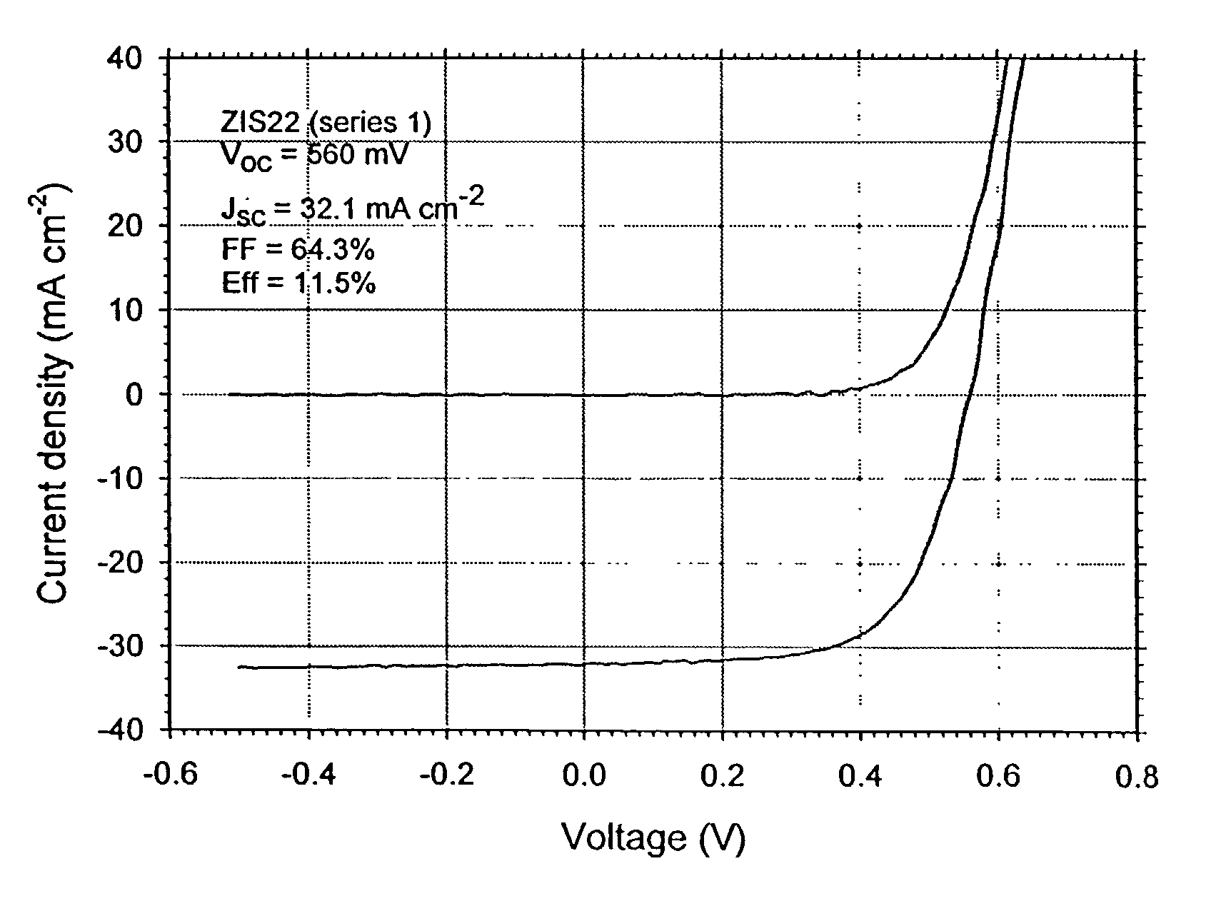
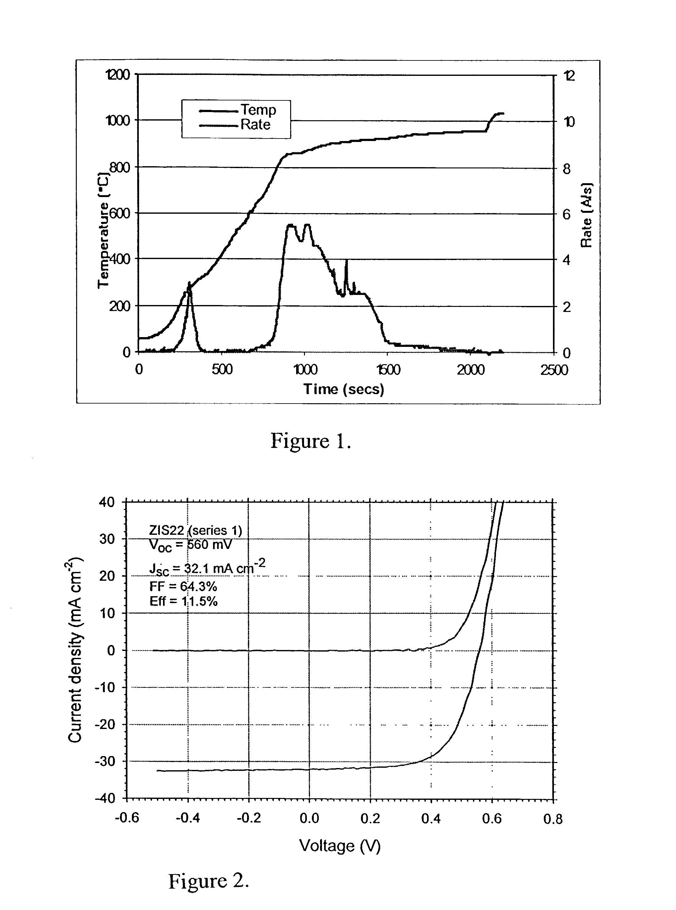
[0057]This example describes the fabrication of the solar cell reported in run 51 of Table 1. The starting sample consists of a piece of glass bearing a sputtered Mo back contact and a film of CIGS of about 2.5 μm in thickness. The sample was rinsed in de-ionized water for one minute, dried in a stream of nitrogen, and mounted in a vacuum evaporator. The source crucible was made of graphite. 10 mg of ZnIn2Se4 (ZIS) was placed in the crucible, together with 19 mg of sulfur. The system was pumped to a pressure of 1.2×10⁻⁶ Torr using a diffusion pump, and the substrate was heated to 185° C. The crucible was heated using a resistive heater causing the evaporation of the sulfur followed by the ZIS. The sample was cooled to about 50° C. before removing it from the chamber. A single layer of transparent and conductive ZnO:Al was sputtered for 9 minutes onto the ZIS. The sample was removed from the sputtering chamber and devices were defined by mechanical scribing. The devices (solar cells)...


PUM


Abstract

Sulfur is used to improve the performance of CIGS devices prepared by the evaporation of a single source ZIS type compound to form a buffer layer on the CIGS. The sulfur may be evaporated, or contained in the ZIS type material, or both. Vacuum evaporation apparatus of many types useful in the practice of the invention are known in the art. Other methods of delivery, such as sputtering, or application of a thiourea solution, may be substituted for evaporation.

Description

PRIORITY[0001]This application claims priority from Provisional Application Ser. No. 60 / 331,867, filed Nov. 20, 2001.GOVERNMENT SPONSORED RESEARCH[0002]This invention was made with government support under NREL Subcontract No. ZAK-8-17619-21, Prime Contract No. DE-AC36-99GO10337 awarded by the Department of Energy. The government has certain rights in this invention.BACKGROUND OF THE INVENTION[0003]1. Field of the Invention[0004]The invention is in the field of photovoltaic devices, such as solar cells.[0005]2. Brief Description of the Background Art[0006]Chalcopyrite semiconductors based on CuInSe2 (or CIS) have been investigated for their application to thin film solar cells for over 25 years. Chalcopyrite semiconductors are formed from group I, group III, and group VI elements of the periodic table. Alloying of CuInSe2 and CuGaSe2 to form Cu(InxGa1-x)Se2 (or CIGS) allows the energy gap to be varied between 1.0 eV and 1.68 eV in order to vary the spectral absorption profile. Alloy...

Claims


Application Information

Patent Timeline
Patent Type & Authority Patents(United States)
IPC IPC(8): H01L31/0264H01L31/0272H01LH01L31/00H01L31/032
CPCH01L31/0322Y02E10/541
Inventor DELAHOY, ALAN E.
Owner NEW MILLENNIUM SOLAR EQUIP CORP
Why Eureka
Try Eureka