Current inrush limiting circuit

Inactive Publication Date: 2006-03-28
COGNITIVETPG
View PDF15 Cites 33 Cited by
  • Summary
  • Abstract
  • Description
  • Claims
  • Application Information

AI Technical Summary

Benefits of technology

[0010]In accordance with the present invention, there is provided a circuit for limiting hot-plug or DC-side power switched inrush current into electronic devices having high input capacitance. The circuit applies an active feedback-controlled voltage ramp to a bulk capacitor by means of a P-channel field effect transistor that is operated linearly after a controlled delay for contact bounce. Linear output voltage ramp to the load capacitor is ensured by providing active control of the gate voltage, via an operational amplifier with voltage feedback. The ramp is generated by an RC network, but only the first third of the exponential is used, wherein the waveshape is quite linear and approaches that of an ideal ramp. Since a voltage ramp applied to a capacitor implies constant current, the inrush current is controlled to the extent that the ramp is linear. To ensure the initial state is OFF, and the final state is Full-On, gain is applied in the feedback loop, wherein the reference voltage ramp drives the FET via the op a

Problems solved by technology

This method has the disadvantage of added cost of the resistor or thermistor that must pass the inrush current.
Such a scheme is also limited by long turn-on delays, in order to ensure safe operation of the system.
Such schemes are also limited to situations where exact capacitor value is known.
While this approach can work better over a greater parts variation

Method used


Image

  • Current inrush limiting circuit
  • Current inrush limiting circuit
  • Current inrush limiting circuit

Examples


Embodiment Construction

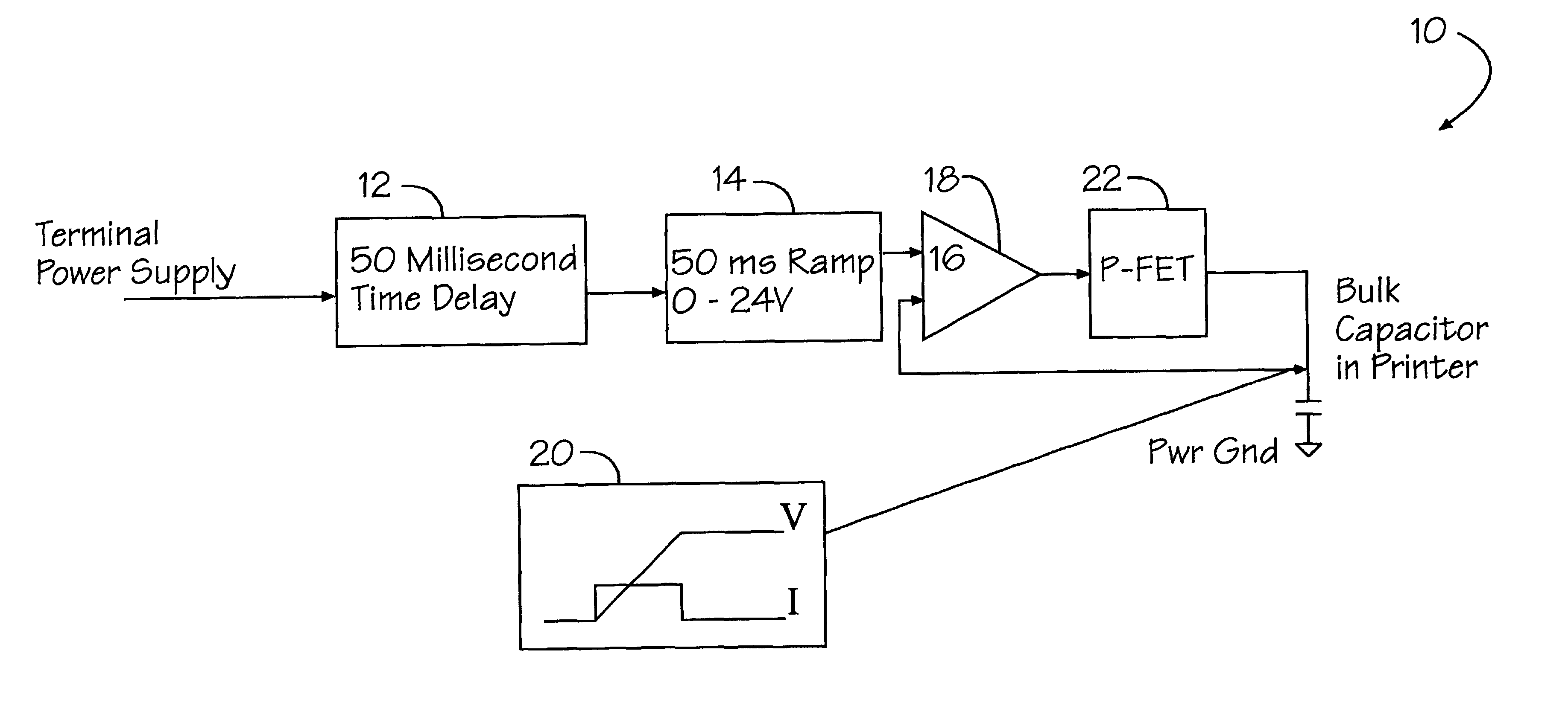
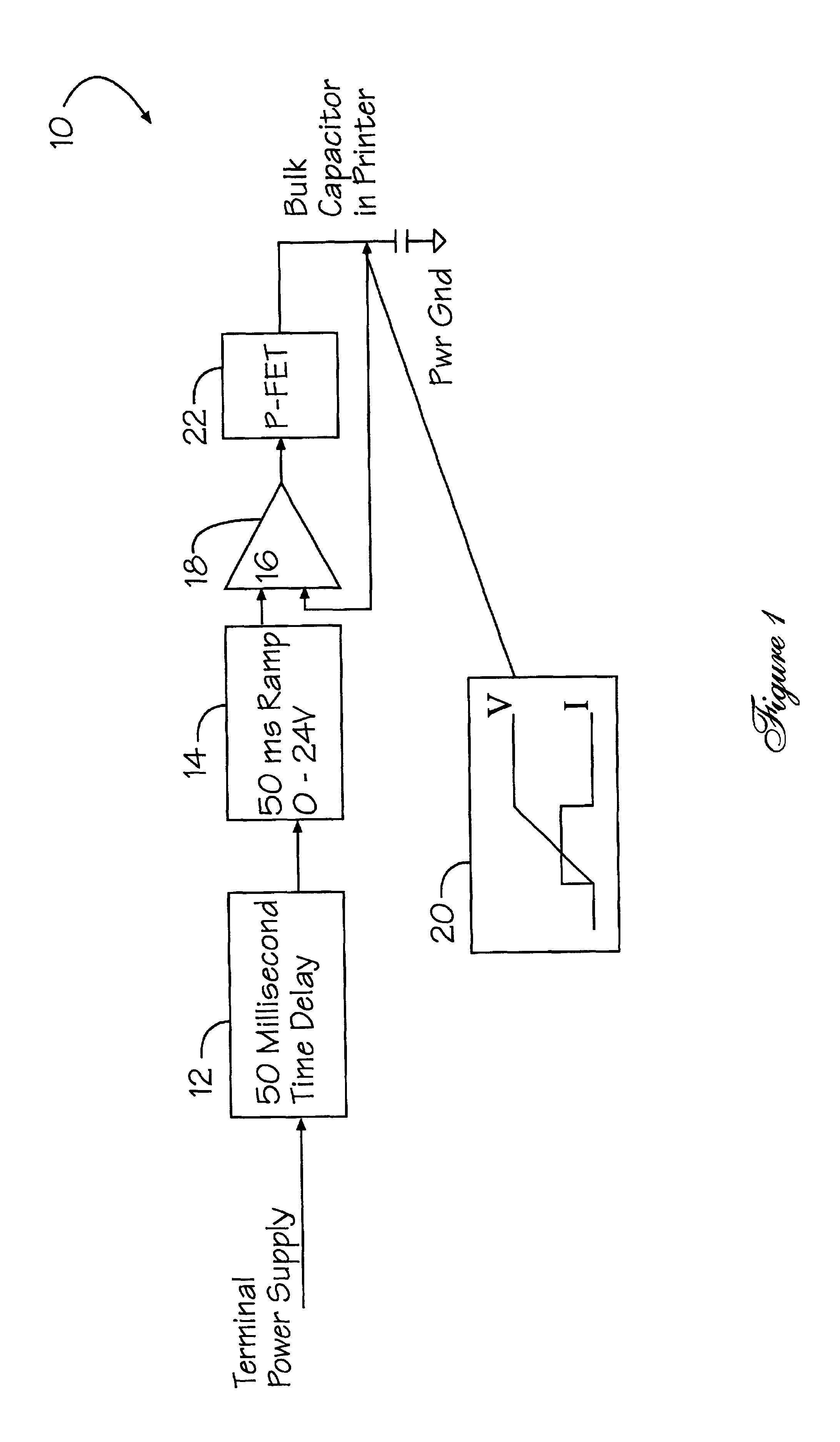
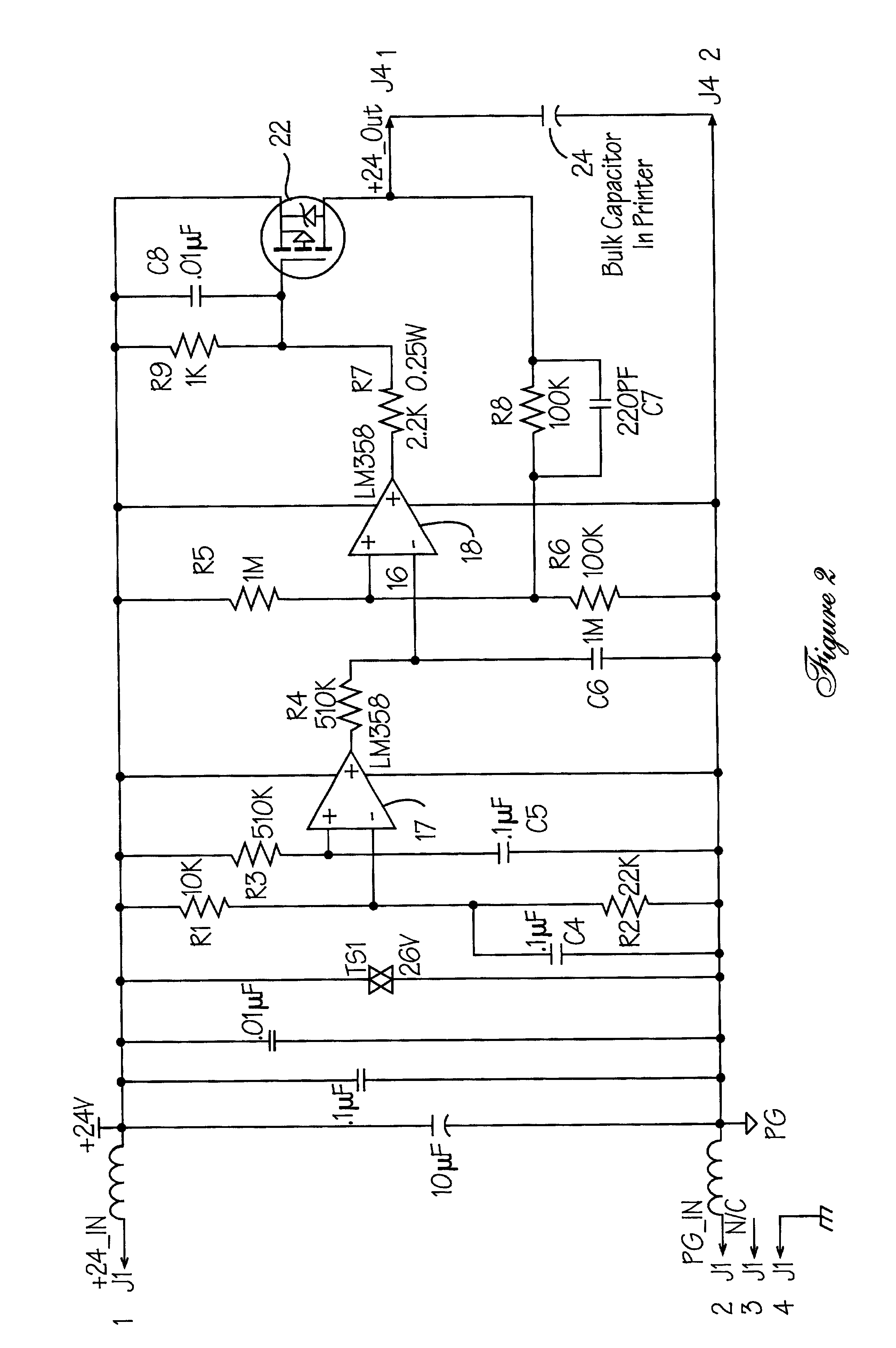
[0017]Generally speaking, the invention features an inrush circuit for electronic devices and, in particular, an inrush circuit for point-of-sale printers. The circuit limits hot-plug or DC-side power switched inrush current into devices having high input capacitance. The circuit applies an active feedback-controlled voltage ramp to a bulk capacitor by means of a P-channel field effect transistor that is operated linearly after a controlled delay for contact bounce. Linear output voltage ramp to the load capacitor is ensured by providing active control of the gate voltage, via an operational amplifier with voltage feedback. The ramp is generated by an RC network, but only the first third of the exponential is used, wherein the waveshape is linear and approaches that of an ideal ramp. Since a voltage ramp applied to a capacitor implies constant current, the inrush current is controlled to the extent that the ramp is linear.

[0018]Now referring to FIG. 1, a block diagram of the inrush ...


PUM


Abstract

An inrush circuit for electronic devices is particularly useful for point-of-sale printers. The circuit applies an active feedback-controlled voltage ramp to a bulk capacitor by means of a P-channel field effect transistor that is operated linearly after a controlled delay for contact bounce.

Description

FIELD OF THE INVENTION[0001]The present invention relates to circuits for limiting hot-plug or DC-side power switched inrush current and, more particularly, to an inrush limiting circuit that comprises four subsystems that cooperate with each other to effectively eliminate large inrush currents regardless of the cycle time of the device being powered or its input capacitance.BACKGROUND OF THE INVENTION[0002]Circuit boards, or devices containing large power supply bulk capacitance, experience an uncontrolled initial inrush current that charges the capacitance when power is initially applied. This inrush current can cause damage to components, system disruption or permanent failure thereof.[0003]Recent tests have shown that various point-of-sale (POS) printers have inrush current that is not properly limited. Often, attempts to resolve the problem have been primitive, and have been only marginally successful. In addition, many of these previous attempts to deal with this problem have ...

Claims


Application Information

Patent Timeline
IPC IPC(8): G05F1/10G05F3/02H02H9/00
CPCH02H9/001Y10S323/908
Inventor DEL SIGNORE, II, JAMES R.SPANO, STEVEN M.BULLOCK, RANDOLPH
Owner COGNITIVETPG
Why Eureka
Try Eureka