Semiconductor thin film and process for production thereof

Active Publication Date: 2006-04-04
PANASONIC LIQUID CRYSTAL DISPLAY CO LTD +1
View PDF6 Cites 19 Cited by
  • Summary
  • Abstract
  • Description
  • Claims
  • Application Information

AI Technical Summary

Benefits of technology

[0012]The present invention was completed in view of the foregoing. It is an object of the present invention to provide a process for efficiently forming a silicon thi

Problems solved by technology

The result is that there remain regions in which crystallization is incomplete.
A disadvantage of linear beam is th

Method used


Image

  • Semiconductor thin film and process for production thereof
  • Semiconductor thin film and process for production thereof
  • Semiconductor thin film and process for production thereof

Examples


example 1

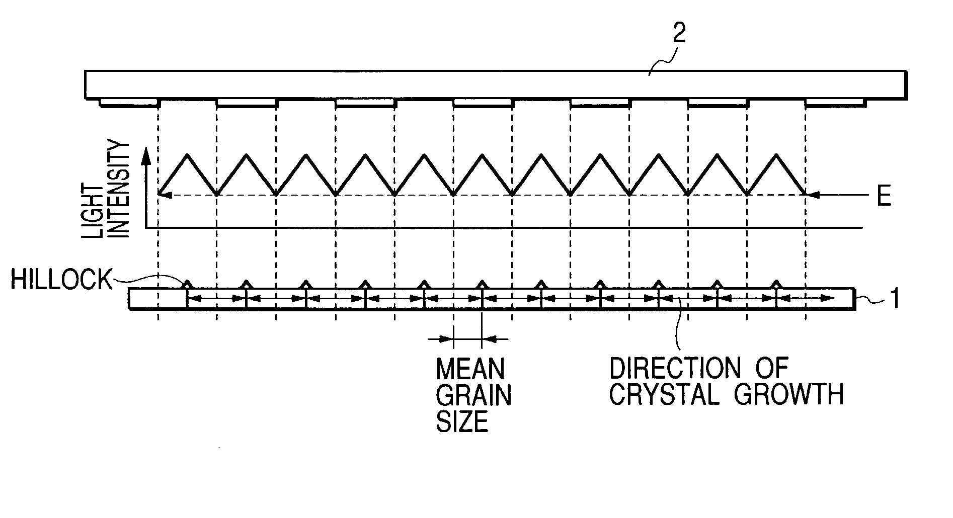
[0062]The laser annealing process according to the present invention is accomplished by using an apparatus shown in FIG. 13. There is shown a sample substrate 1 having an amorphous silicon film formed thereon. There is also shown a mask 2 which is placed 0.6 mm above the substrate 1. This mask is a periodic phase-shifting mask with a stripy pattern scribed at a pitch of 2 μm. (An enlarged side view of the substrate 1 and the mask 2 is shown in FIG. 1.) There is shown a pulsed laser beam 3 specified below.[0063]XeCl Excimer Laser Generated by Model STEEL 1000 of Lamda Physik Corporation.[0064]Wavelength: 308 nm[0065]Pulse intervals: approx. 27 ns[0066]Repeating frequency: 300 Hz

The laser beam 3 is shaped into a linear beam, 365 mm in long axis and 400 μm in short axis, by an optical system consisting of a homogenizer 7 (from Micro Las Corporation) and cylindrical lenses 6 and 5. There is shown a substrate stage 4 which feeds the substrate at a prescribed rate during laser irradiation...

example 2

[0072]This example uses the same equipment as in Example 1 but differs in the way of irradiation. In this example, irradiation may be carried out in two steps. Irradiation in the first step is through a mask pattern as with the foregoing embodiment, and no mask pattern is used for irradiation in the second step. Irradiation in this manner yields a thin film consisting of isotropic crystal grains and having low hillocks. Alternatively, irradiation may be carried out such that no mask pattern is used in the first step and a mask pattern is used in the second step. The effect of irradiation in this manner is that the second step (with a mask pattern) ensures crystallization at the part where the light intensity is very low. This effect permits the process to be run with low laser energy.

example 3

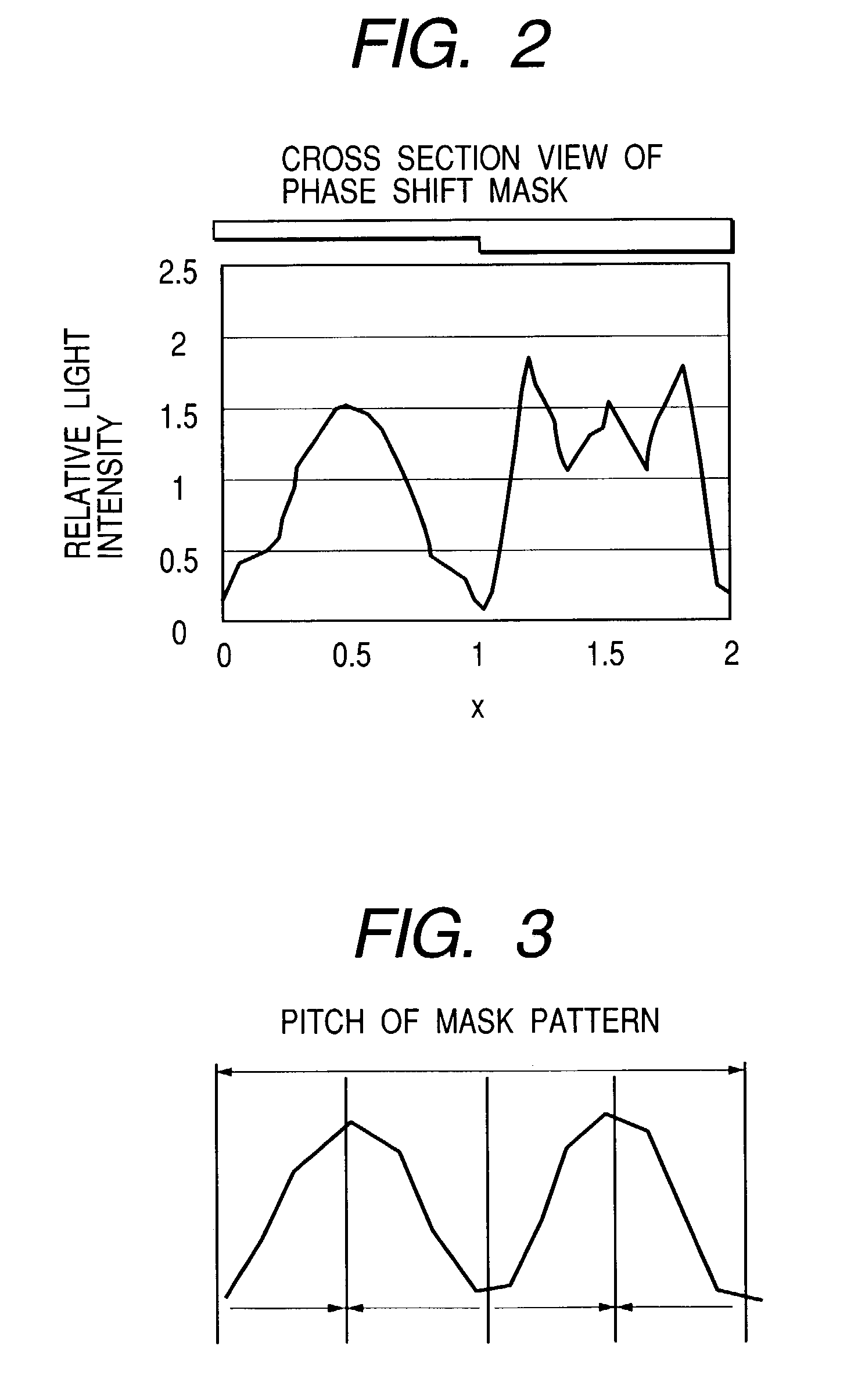
[0073]This example uses the same equipment as in Example 1 except for the phase-shifting mask in which the stripy pattern has a pitch of 3 μm. In this example, the mask is 0.9 mm away from the substrate and the rate of scanning is 30 mm / s for 4-shot overlapping. Scanning is carried out in a direction which is aslant about 0.17 degrees with respect to the mask so that the shift of the pattern is 0.2 μm as shown in FIG. 6. This is because the interval of hillocks is 1.5 μm and hence the shift should be smaller than 0.325 μm (1.5 μm divided by 4) for 4 shots on the same spot. Thus, repeating overlapping shots four times with a specific amount of shift reduces hillocks.


PUM


Abstract

To improve the laser annealing process for polycrystallizing amorphous silicon to form silicon thin films having large crystal particle diameters at a high throughput, the present invention is directed to a process of crystallization by irradiation of a semiconductor thin film formed on a substrate with pulsed laser light. The process comprises having a means to shape laser light into a linear beam and a means to periodically and spatially modulate the intensity of pulsed laser in the direction of the long axis of the linear beam by passing through a phase-shifting stripy pattern perpendicular to the long axis, and collectively forming for each shot a polycrystalline film composed of crystals which have grown in a certain direction over the entire region irradiated with the linear beam.

Description

BACKGROUND OF THE INVENTION[0001]1. Field of the Invention[0002]The present invention relates to a semiconductor thin film and a process for production thereof. It is applicable to semiconductor devices including polysilicon thin film transistors (for liquid crystal displays), solar cells, and SOI devices.[0003]2. Description of Related Art[0004]A liquid crystal display has thin film transistors (TFTs) as driving devices. The active layer of TFTs is dominated by polysilicon (poly-Si) film rather than amorphous silicon (a-Si) film, because the former permits carriers (electrons in n-channel and holes in p-channel) high mobility and helps realize smaller cells for a fine pitch display. Another advantage of poly-Si film is the capability of low-temperature annealing by laser. This technique, unlike ordinary annealing that needs a high-temperature process (at 1000° C. or above), prevents the substrate from getting hot during annealing and hence permits TFTs to be formed on an inexpensiv...

Claims


Application Information

Patent Timeline
IPC IPC(8): C30B23/00C30B13/00H01L21/20H01L21/336H01L29/786
CPCC30B13/00C30B29/06Y10S117/904
Inventor TAKEDA, KAZUOGOTOU, JUNSAITO, MASAKAZUOHKURA, MAKOTOSATOU, TAKESHIFUKUDA, HIROSHISHIBA, TAKEO
Owner PANASONIC LIQUID CRYSTAL DISPLAY CO LTD
Why Eureka
Try Eureka