
Near-field exposure photoresist and fine pattern forming method using the same

a technology of near-field exposure and fine pattern forming, which is applied in the direction of photosensitive materials, instruments, photomechanical equipment, etc., can solve the problems of reducing process tolerance, failure of transfer onto the substrate, and increasing the width of the formed pattern, and achieves high contrast

Inactive Publication Date: 2006-04-04
CANON KK
View PDF20 Cites 19 Cited by
  • Summary
  • Abstract
  • Description
  • Claims
  • Application Information

AI Technical Summary

Benefits of technology

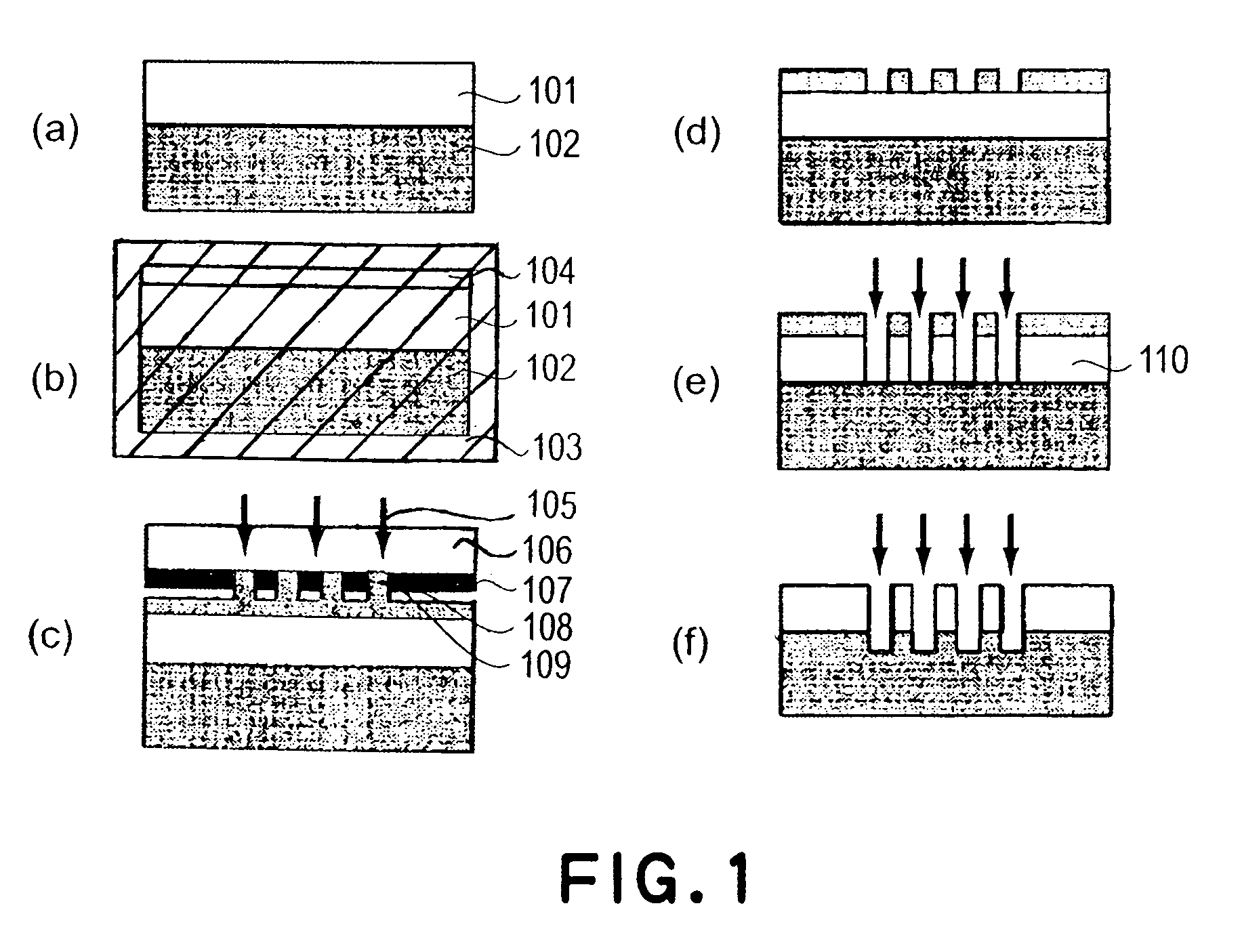
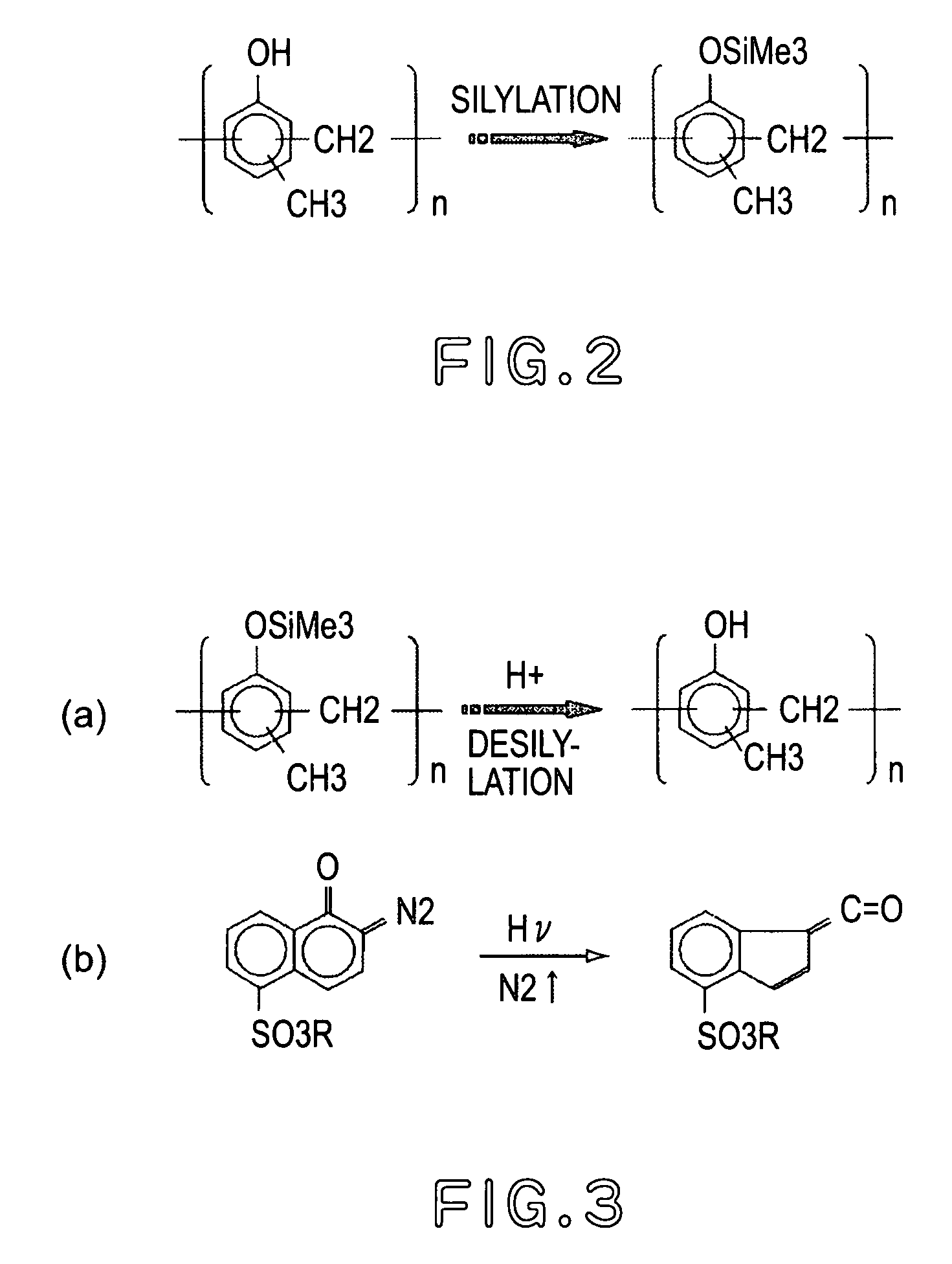
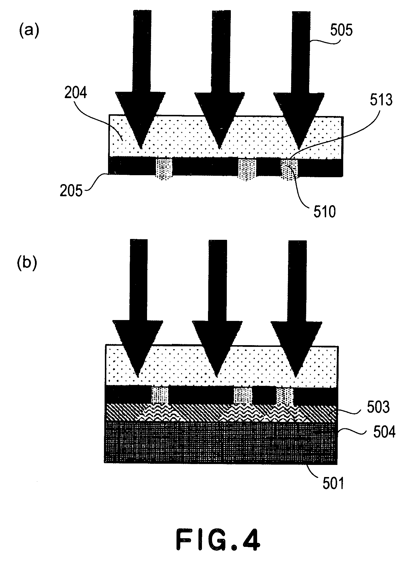
The present invention provides a near-field exposure photoresist that can transfer a resist pattern with high contrast and a high aspect ratio onto a workpiece substrate with process tolerance. The photoresist includes an alkali-soluble novolac resin, a diazide-type photosensitizer, a photoacid generator, and a solvent. The invention also provides a fine pattern forming method using the near-field exposure photoresist, which includes steps of preparing the exposure mask, preparing the photoresist, disposing the photoresist on the workpiece substrate, silylating the photoresist, forming a fine pattern, and transferring the pattern onto the substrate. The thickness of the silylated portion is preferably not more than a size of an opening diameter of a small opening of a mask for use in near-field exposure.

Problems solved by technology

However, in order to effect further fine patterning, there are many problems to be solved, such as a shorter wavelength of laser light, development of lens which can be used in such a shorter wavelength region, and a compact apparatus.
However, a photoresist is exposed to scattered light which is created by disturbing near-field light by the photoresist, so that a resultant width of a formed pattern is increased when the thickness of the photoresist for image formation is large.
Accordingly, when a finer pattern is formed, there is a possibility that a process tolerance is lowered during the pattern transfer onto the substrate or that the pattern transfer onto the substrate is failed with respect to such a substrate that it requires the use of gas or system providing an insufficient latitude in selection of the photoresist.

Method used


Image

  • Near-field exposure photoresist and fine pattern forming method using the same
  • Near-field exposure photoresist and fine pattern forming method using the same
  • Near-field exposure photoresist and fine pattern forming method using the same

Examples


example

[0071]In order to form a 50 nm L / S (line and space) pattern of a 100 nm-thick upper Si layer on SiO2 layer of SOI (silicon on insulator) substrate, a photoresist was formed on the SOI substrate by spin coating.

[0072]The photoresist contained an alkali-soluble novalac resin, a photosensitizer having a naphthoquinonediazide group, triazine and a sensitizer.

[0073]With respect to the thickness of the photoresist layer, it is necessary to provide the photoresist layer on the SOI substrate with a thickness of to less than 50 nm in view of a ratio of etching resistance between Si and the photoresist with respect to a mixture gas of CHF3 and SF6 since Si is etched with the mixture gas. Further, in order to form the 50 nm L / S pattern by near-field exposure, a width of a small opening of the photomask used in the near-field exposure is approximately 20 nm. For this reason, a thickness of the silylation portion is determined as 20 nm.

[0074]When a 20 nm-thick silylation portion is used as the p...


PUM

PropertyMeasurementUnit
wavelengthaaaaaaaaaa
temperatureaaaaaaaaaa

Abstract

A near-field photoresist for formation of a fine pattern with by near-field exposure includes an alkali-soluble novalac resin, a diazyde-type photosensitizer which is photoreactive by near-field exposure, a photoacid generator which generates acid by the near-field exposure, and a solvent.

Description

FIELD OF THE INVENTION AND RELATED ART[0001]The present invention relates to an near-field exposure photoresist and a fine pattern forming method using the near-field exposure photoresist.[0002]In recent years, with the progress of an increase in capacity of a semiconductor memory and a high-speed and high-integrated CPU (central processing unit), smaller photolithography has been further required. For this purpose, a wavelength of light used in a photolithographic apparatus is made shorter, and a ultraviolet laser has been presently used, thus permitting fine patterning of about 0.1 μm. However, in order to effect further fine patterning, there are many problems to be solved, such as a shorter wavelength of laser light, development of lens which can be used in such a shorter wavelength region, and a compact apparatus.[0003]On the other hand, a method using near-field light has been proposed in order to effect formation of a photoresist pattern having a width of not more than a ligh...

Claims


Application Information

Patent Timeline
Patent Type & Authority Patents(United States)
IPC IPC(8): G03F7/30G03F7/023G03C5/18G03F7/004G03F7/022G03F7/16G03F7/20G03F7/38G03F7/40H01L21/027
CPCG03F7/0226G03F7/0236G03F7/0752G03F7/168G03F7/2014
Inventor YAMAGUCHI, TAKAKOKURODA, RYO
Owner CANON KK
Learn More