Compact system module with built-in thermoelectric cooling

a technology of thermoelectric cooling and compact system modules, applied in the field of compact system modules with built-in thermoelectric cooling, can solve the problems of increasing the number of linked transistors, difficult with today's technology to implement a truly high-performance “system on a chip”, and several problems, which remain inherent in the design structure, to achieve the effect of improving the cooling of high frequency, high-speed microprocessor chip components and increasing the operational bandwidth

Inactive Publication Date: 2006-04-04
MICRON TECH INC
View PDF87 Cites 38 Cited by
  • Summary
  • Abstract
  • Description
  • Claims
  • Application Information

AI Technical Summary

Benefits of technology

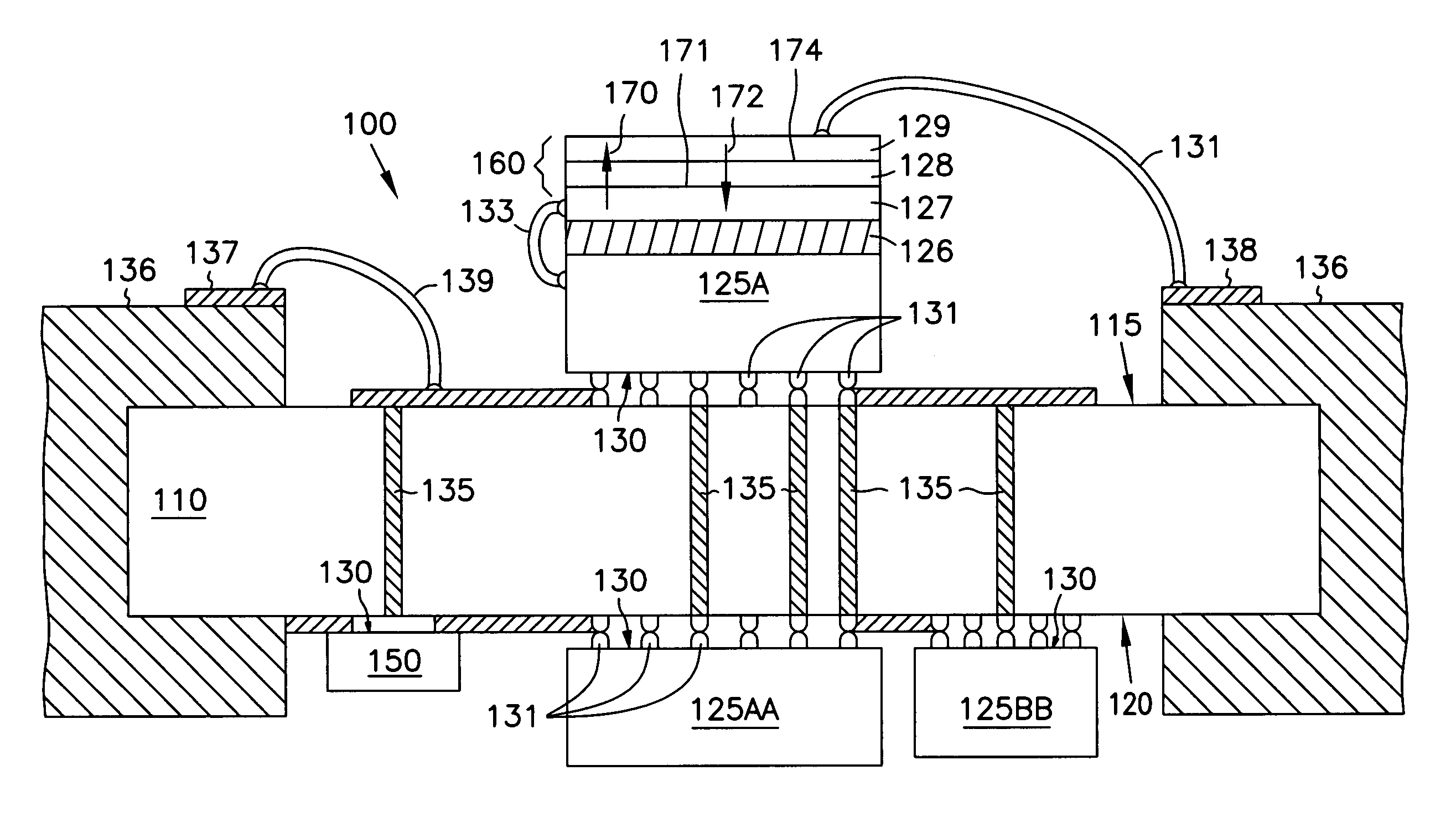
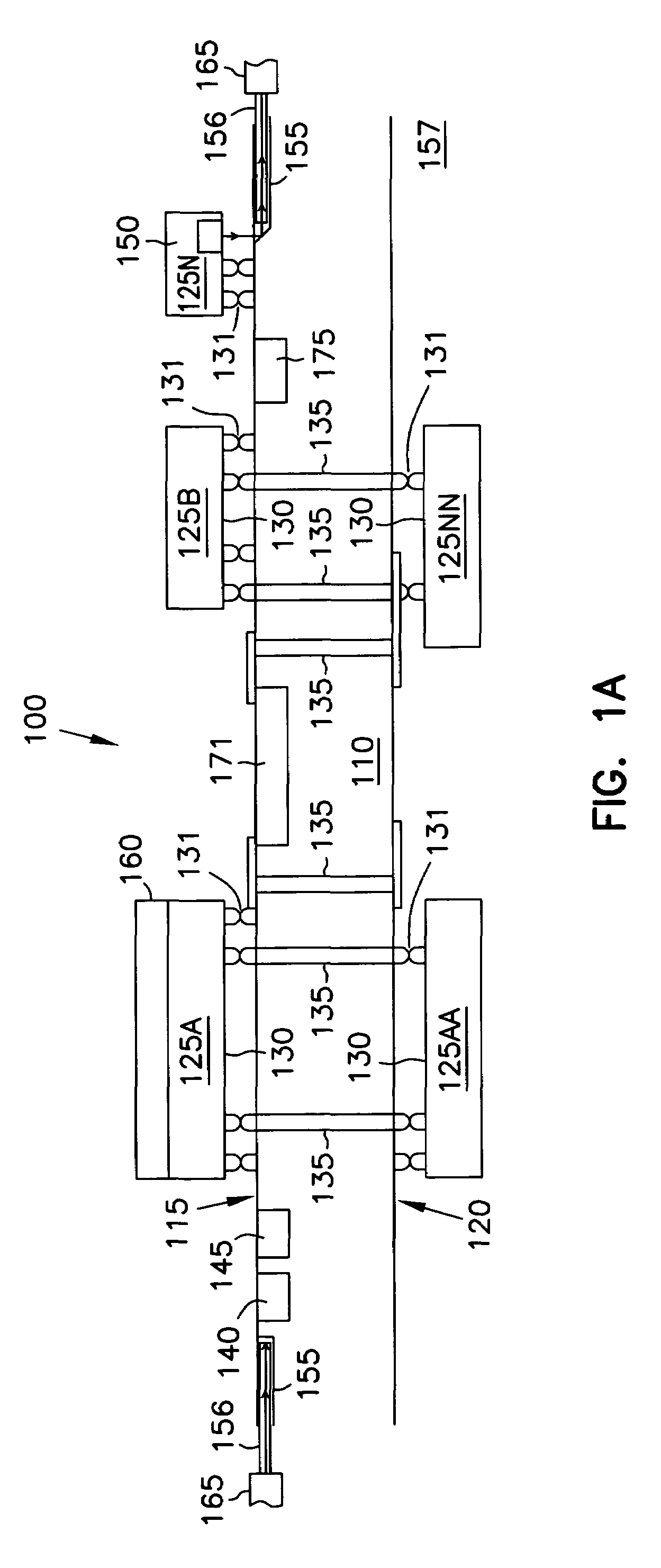
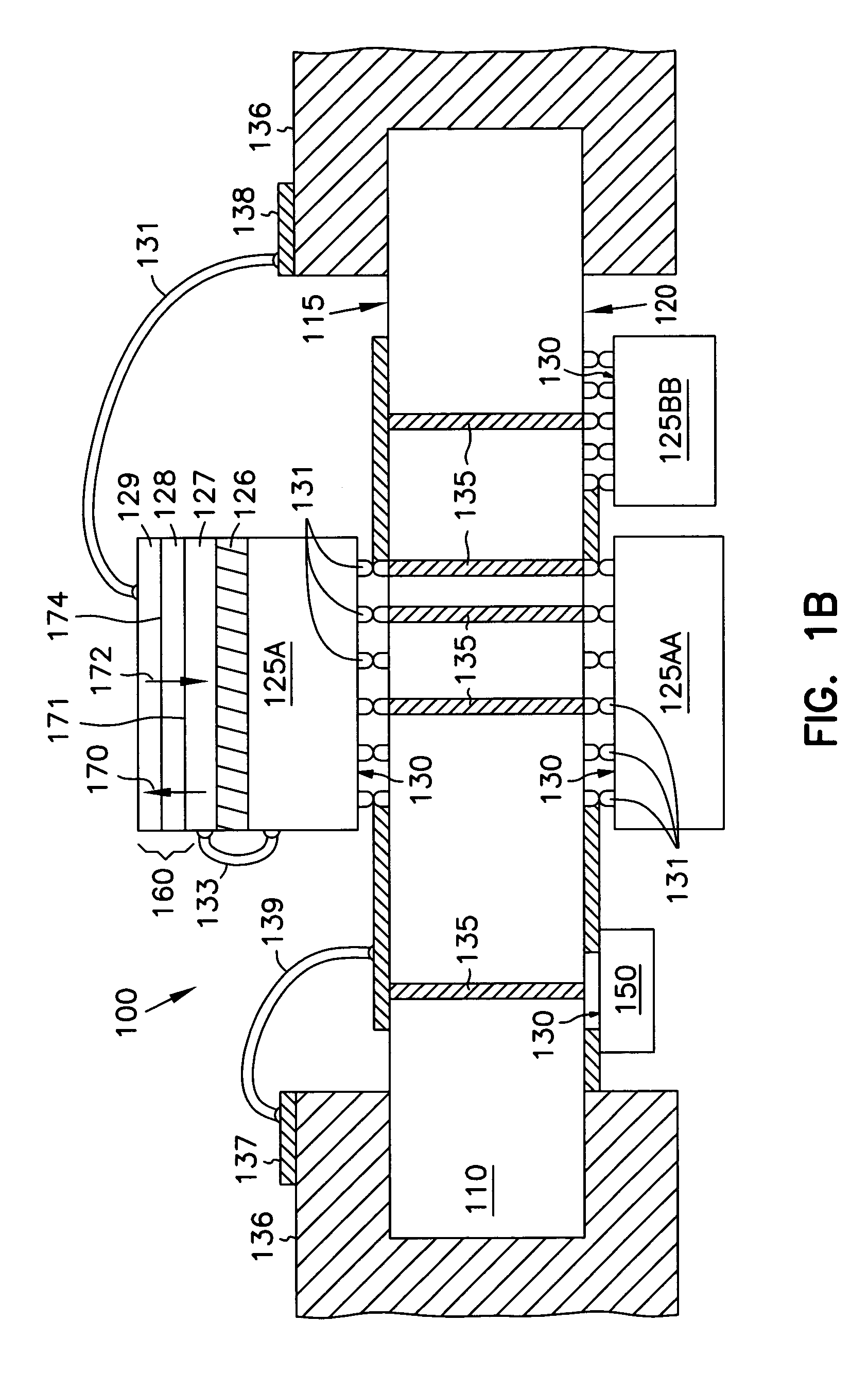
[0009]In particular, an improved integrated circuit package for providing built-in heating or cooling to a semiconductor chip is provided. The improved integrated circuit package provides increased operational bandwidth between different circuit devices, e.g. logic and memory chips. The improved integrated circuit package does not require changes in current CMOS processing techniques. The structure includes the use of a silicon interposer. The silicon interposer can consist of recycled rejected wafers from the front-end semiconductor processing. Micro-machined vias are formed through the silicon interposer. The micro-machined vias include electrical contacts which couple various integrated circuit devices located on the opposing surfaces of the silicon interposer. The packaging includes a Peltier element.
[0010]The Peltier element, using semiconductor-based materials, functions as a small heat pump. By applying a low-voltage d-c current to the Peltier element thermal energy is transferred with the effect that one portion of the Peltier element is cooled and another heated. In one embodiment, the heated portion of the Peltier element is in contact with a heat sink or the outer cover of the integrated circuit package and the cooled portion is in contact with a semiconductor chip. Thus providing improved cooling for high frequency, high speed microprocessor chip components. In an alternative embodiment, the arrangement is reversed. This design has no moving parts, is small in size and lightweight, and has the ability to cool below or heat above the ambient temperature surrounding integrated circuit devices.

Problems solved by technology

The complexity of these circuits requires the use of an ever increasing number of linked transistors.
Unfortunately, it is very difficult with today's technology to implement a truly high-performance “system on a chip” because of vastly different fabrication processes and different manufacturing yields for the logic and memory circuits.
Several problems, however, remain inherent with this design structure.
One serious complication includes the heating which occurs most seriously in connection with a logic chip such as a microprocessor.
In high-performance microprocessors, where CPUs are running at 500 MHz and dissipating up to 85 watts of power, cooling becomes a crucial issue.
In certain applications, however, forced air cooling is not feasible or practical.
Still, liquid cooling methods can also prove too bulky, costly, and not easily adapted for use in compact high-performance integrated circuit systems, e.g. portable devices.

Method used


Image

  • Compact system module with built-in thermoelectric cooling
  • Compact system module with built-in thermoelectric cooling
  • Compact system module with built-in thermoelectric cooling

Examples


Embodiment Construction

[0022]In the following detailed description of the invention, reference is made to the accompanying drawings which form a part hereof, and in which is shown, by way of illustration, specific embodiments in which the invention may be practiced. In the drawings, like numerals describe substantially similar components throughout the several views. These embodiments are described in sufficient detail to enable those skilled in the art to practice the invention. Other embodiments may be utilized and structural, logical, and electrical changes may be made without departing from the scope of the present invention.

[0023]The terms wafer and substrate used in the following description include any structure having an exposed surface with which to form the integrated circuit (IC) structure of the invention. The term substrate is understood to include semiconductor wafers. The term substrate is also used to refer to semiconductor structures during processing, and may include other layers that ha...


PUM


Abstract

An improved integrated circuit package for providing built-in heating or cooling to a semiconductor chip is provided. The improved integrated circuit package provides increased operational bandwidth between different circuit devices, e.g. logic and memory chips. The improved integrated circuit package does not require changes in current CMOS processing techniques. The structure includes the use of a silicon interposer. The silicon interposer can consist of recycled rejected wafers from the front-end semiconductor processing. Micro-machined vias are formed through the silicon interposer. The micro-machined vias include electrical contacts which couple various integrated circuit devices located on the opposing surfaces of the silicon interposer. The packaging includes a Peltier element.

Description

[0001]This application is a divisional of U.S. application Ser. No. 09 / 144,307 filed on Aug. 31, 1998, now U.S. Pat. No. 6,586,835, which is incorporated herein by reference.FIELD OF THE INVENTION[0002]The present invention relates generally to semiconductor integrated circuits. More particularly, it pertains to a compact system module with built-in thermoelectric cooling.BACKGROUND OF THE INVENTION[0003]Integrated circuit technology relies on transistors to formulate vast arrays of functional circuits. The complexity of these circuits requires the use of an ever increasing number of linked transistors. As the number of transistors required increases, the integrated circuitry dimensions shrink. It is one objective in the semiconductor industry to construct transistors and other discrete devices which occupy less surface area on a given silicon chip / die. At the same time, the semiconductor industry seeks to increase the speed and power offered by integrated circuits. One approach to ...

Claims


Application Information

Patent Timeline
Patent Type & Authority Patents(United States)
IPC IPC(8): H01L21/50H01L21/24H01L21/302H01L23/34H01L27/16H01L23/38H01L23/498H01L25/065
CPCG02B6/4214H01L21/486H01L23/147H01L23/345H01L23/38H01L23/48H01L23/49827H01L24/73H01L25/0652H01L25/16H01L25/50H01L2224/16235H01L25/167H01L33/62H01L33/645H01L2224/16237H01L2224/48227H01L2224/73257H01L2924/01013H01L2924/01029H01L2924/01032H01L2924/01038H01L2924/01051H01L2924/01052H01L2924/01077H01L2924/01078H01L2924/01082H01L2924/10329H01L2924/14H01L2924/19041H01L24/48H01L2924/01006H01L2924/01023H01L2924/01033H01L2924/01045H01L2924/12041Y10S257/93H01L2924/10253G02B6/4232H01L2924/1301H01L2924/19107H01L2224/73265H01L2224/48091H01L2924/00H01L2924/00014H01L2924/12042H01L2224/056H01L2224/45099H01L2224/854H01L2224/16225H01L2924/15173H01L2224/45015H01L2924/207
Inventor AHN, KIE Y.FORBES, LEONARDCLOUD, EUGENE H.
Owner MICRON TECH INC
Why Eureka
Try Eureka