CMOS on hybrid substrate with different crystal orientations using silicon-to-silicon direct wafer bonding

a technology of silicon-to-silicon direct bonding and hybrid substrate, which is applied in the direction of transistors, semiconductor devices, electrical equipment, etc., can solve the problems of significant deformation of electron mobilities on (b>110/b>) si surfaces, undesirable pfets having larger widths, and completely inappropriate crystal orientation for nfet devices, etc., to achieve the effect of improving the performance of each type of devi

Inactive Publication Date: 2006-04-04
GLOBALFOUNDRIES INC
View PDF4 Cites 152 Cited by
  • Summary
  • Abstract
  • Description
  • Claims
  • Application Information

AI Technical Summary

Benefits of technology

[0011]One object of the present invention is to provide a method of integrating semiconductor devices such that different types of devices are formed upon a specific crystal orientation of a hybrid substrate that enhances the performance of each type of device.
[0013]A further object of the present invention is to provide a method of integrating semiconductor devices on a hybrid substrate having different crystal orientations such that each device is a bulk-like device and is located on a crystal orientation which enhances the performance of the device.

Problems solved by technology

To compensate for this discrepancy, pFETs are typically designed with larger widths in order to balance pull-up currents against the nFET pull-down currents and achieve uniform circuit switching. pFETs having larger widths are undesirable since they take up a significant amount of chip area.
Unfortunately, electron mobilities on (110) Si surfaces are significantly degraded compared to (100) Si surfaces.
As can be deduced from the above discussion, the (110) Si surface is optimal for pFET devices because of excellent hole mobility, yet such a crystal orientation is completely inappropriate for nFET devices.

Method used


Image

  • CMOS on hybrid substrate with different crystal orientations using silicon-to-silicon direct wafer bonding
  • CMOS on hybrid substrate with different crystal orientations using silicon-to-silicon direct wafer bonding
  • CMOS on hybrid substrate with different crystal orientations using silicon-to-silicon direct wafer bonding

Examples


Embodiment Construction

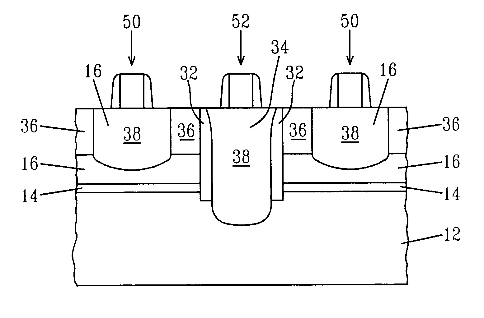
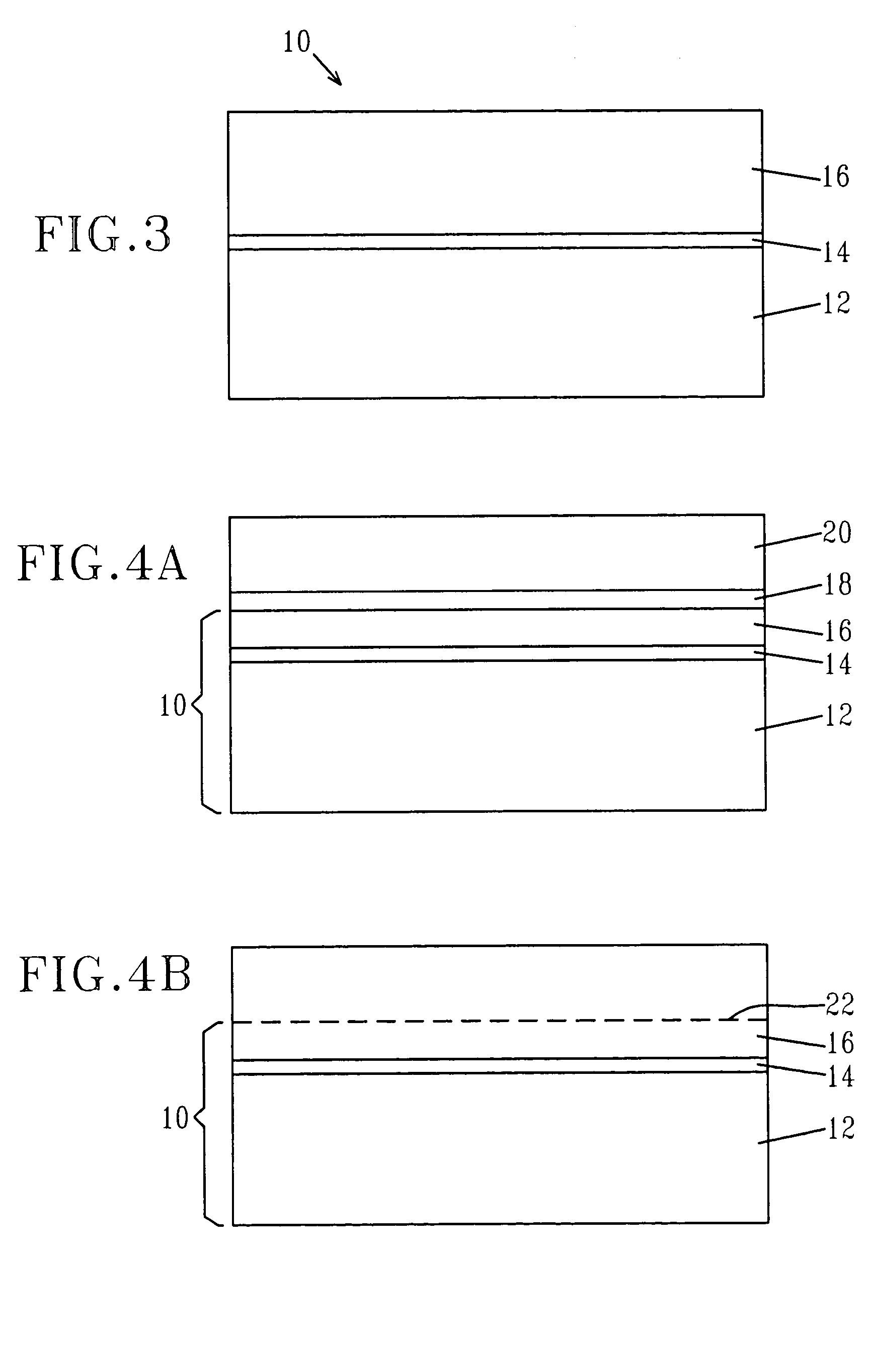
[0044]The present invention, which provides a method of forming CMOS devices on a hybrid substrate having different crystal orientations using semiconductor-to-semiconductor direct bonding, will now be described in more detail by referring to the drawings that accompany the present application.

[0045]FIG. 3 shows an initial hybrid substrate 10 having different crystallographic orientations that can be employed in the present invention. Specifically, the hybrid substrate 10 includes a first (bottom) semiconductor layer 12 and a second (top) semiconductor layer 16 having a bonding interface 14 located therebetween. In accordance with the present invention, the first semiconductor layer 12 comprises a first semiconductor material that has a first crystallographic orientation and the second semiconductor layer 16 comprises a second semiconductor material that has a second crystallographic orientation which differs from the first crystallographic orientation.

[0046]The first semiconductor ...


PUM


Abstract

A method in which semiconductor-to-semiconductor direct wafer bonding is employed to provide a hybrid substrate having semiconductor layers of different crystallographic orientations that are separated by a conductive interface is provided. Also provided are the hybrid substrate produced by the method as well as using the direct bonding method to provide an integrated semiconductor structure in which various CMOS devices are built upon a surface orientation that enhances device performance.

Description

RELATED APPLICATIONS[0001]This application is related to co-pending and co-assigned U.S. patent application Ser. No. 10 / 250,241, filed Jun. 17, 2003, the entire content of which is incorporated herein by reference.FIELD OF THE INVENTION[0002]The present invention relates to high-performance metal oxide semiconductor field effect transistors (MOSFETs) for digital or analog applications, and more particularly to MOSFETs utilizing carrier mobility enhancement from surface orientation.BACKGROUND OF THE INVENTION[0003]In present semiconductor technology, CMOS devices, such as nFETs or pFETs, are typically fabricated upon semiconductor wafers, such as Si, that have a single crystal orientation. In particular, most of today's semiconductor devices are built upon Si having a (100) crystal orientation.[0004]Electrons are known to have a high mobility for a (100) Si surface orientation, but holes are known to have high mobility for a (110) surface orientation. That is, hole mobility values on...

Claims


Application Information

Patent Timeline
Patent Type & Authority Patents(United States)
IPC IPC(8): H01L29/04H01L21/8238H01L21/762
CPCH01L21/76254H01L21/823878H01L21/823807
Inventor IEONG, MEIKEIREZNICEK, ALEXANDERYANG, MIN
Owner GLOBALFOUNDRIES INC
Why Eureka
Try Eureka