Semiconductor integrated circuit device

a technology of integrated circuits and semiconductors, applied in semiconductor devices, semiconductor/solid-state device details, electrical apparatus, etc., can solve the problems of extremely large number of vacuum holes, and achieve the effects of reducing stress, rapid growth, and shortening tim

Inactive Publication Date: 2006-04-04
RENESAS ELECTRONICS CORP
View PDF6 Cites 13 Cited by
  • Summary
  • Abstract
  • Description
  • Claims
  • Application Information

AI Technical Summary

Benefits of technology

[0008]In case of forming plural layers of wiring lines with use of a copper material, first buried wiring lines of a lower layer (“first buried wiring line(s)” hereinafter) are formed, then polishing residues of the copper material present on surfaces of the first-buried wiring lines are removed for preventing the deterioration of a time dependent dielectric breakdown (TDDB) characteristic between adjacent first buried wiring lines, and thereafter the surfaces are modified, for example, by removing gas, moisture and organic matters adhered to the surfaces with use of ammonia plasma, to form highly reliable buried wiring lines. Subsequently, for preventing diffusion of the copper material which forms the first buried wiring lines to an insulating film in which buried wiring lines of an upper layer (“second buried wiring line(s)” hereinafter) are formed and for preventing the exertion of a bad influence of the diffused copper material on the device characteristic, there is formed, for example as a copper material diffusion preventing film, a cap insulating film such as silicon nitride film on the first buried wiring lines. Next, an insulating film such as a silicon oxide film is deposited on the silicon nitride film, then, this insulating film and the cap insulating film are etched to form wiring grooves for formation of the second buried wiring lines and also form connection holes reaching the first buried wiring lines. Thereafter, a copper material is buried into the wiring grooves and the connection holes to form plugs which connect to the second and first buried wiring lines. In the film of the first buried wiring lines there are dotted many vacant holes (atom-free holes). Such vacant holes are present in an extremely large number particularly in the case of a plating film. In the presence of such dotted vacant holes, if a semiconductor wafer formed with first and second buried wiring lines is subjected to a high-temperature shelf test (stress migration test), the vacant holes migrate to the region where the cap insulating film is not present, i.e., the plug-first buried wiring interface, so as to relax a thermal stress (this phenomenon will hereinafter be referred to as “stress migration”). When the vacant holes gather into a large void at the plug-first buried wiring interface, there occurs discontinuity between the associated plug and first buried wiring line.
[0009]By improving the buried wiring-forming process the present inventors could attain to some extent a decrease of stress in the interior of the copper material which forms the buried wiring lines and a decrease of occurrence of many vacant holes in the buried wiring lines, but newly found out that in case of the width of an associated first buried wiring line connected to one plug being large, there could occur discontinuity caused by stress migration. This discontinuity defect is apt to occur as the diameter of each connection hole with a plug formed therein becomes smaller with microfabrication. The migration of vacant holes formed in the film of a buried wiring line occurs concentrically in all directions centered on the bottom of a plug connected to the buried wiring line, so the present inventors presume that the larger the number of vacant holes present in the concentric circles, the more rapid the growth of many vacant holes in the film which forms the plug and the buried wiring line and the shorter the time until the occurrence of discontinuity (stress migration life). That is, the present inventors suspect that the larger the width of a first buried wiring line connected to one plug, the easier will be the occurrence of discontinuity caused by stress migration.
[0010]In connection with a semiconductor integrated circuit having plural layers of buried wiring lines, it is an object of the present invention to provide means for preventing the occurrence of discontinuity caused by stress migration at an interface between a plug connected at a bottom thereof to a buried wiring line and the buried wiring line.

Problems solved by technology

Such vacant holes are present in an extremely large number particularly in the case of a plating film.

Method used


Image

  • Semiconductor integrated circuit device
  • Semiconductor integrated circuit device
  • Semiconductor integrated circuit device

Examples


first embodiment

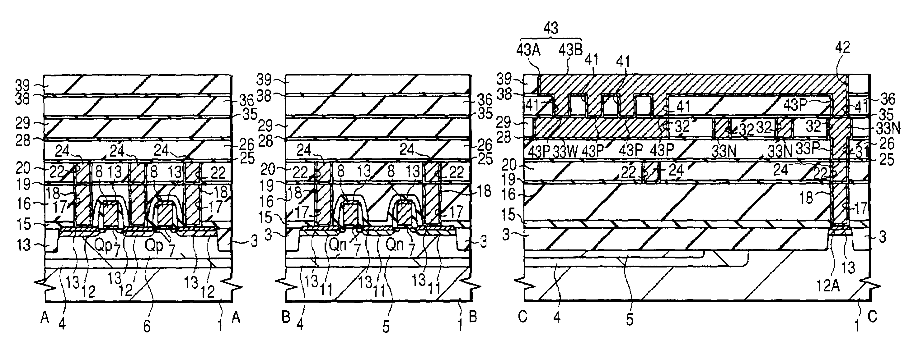
[0131]A semiconductor integrated circuit device according to a first embodiment of the present invention is, for example, a CMOS (Complementary-Metal-Oxide-Semiconductor)-LSI. A method for manufacturing the semiconductor integrated circuit device will be described below in order of manufacturing steps.

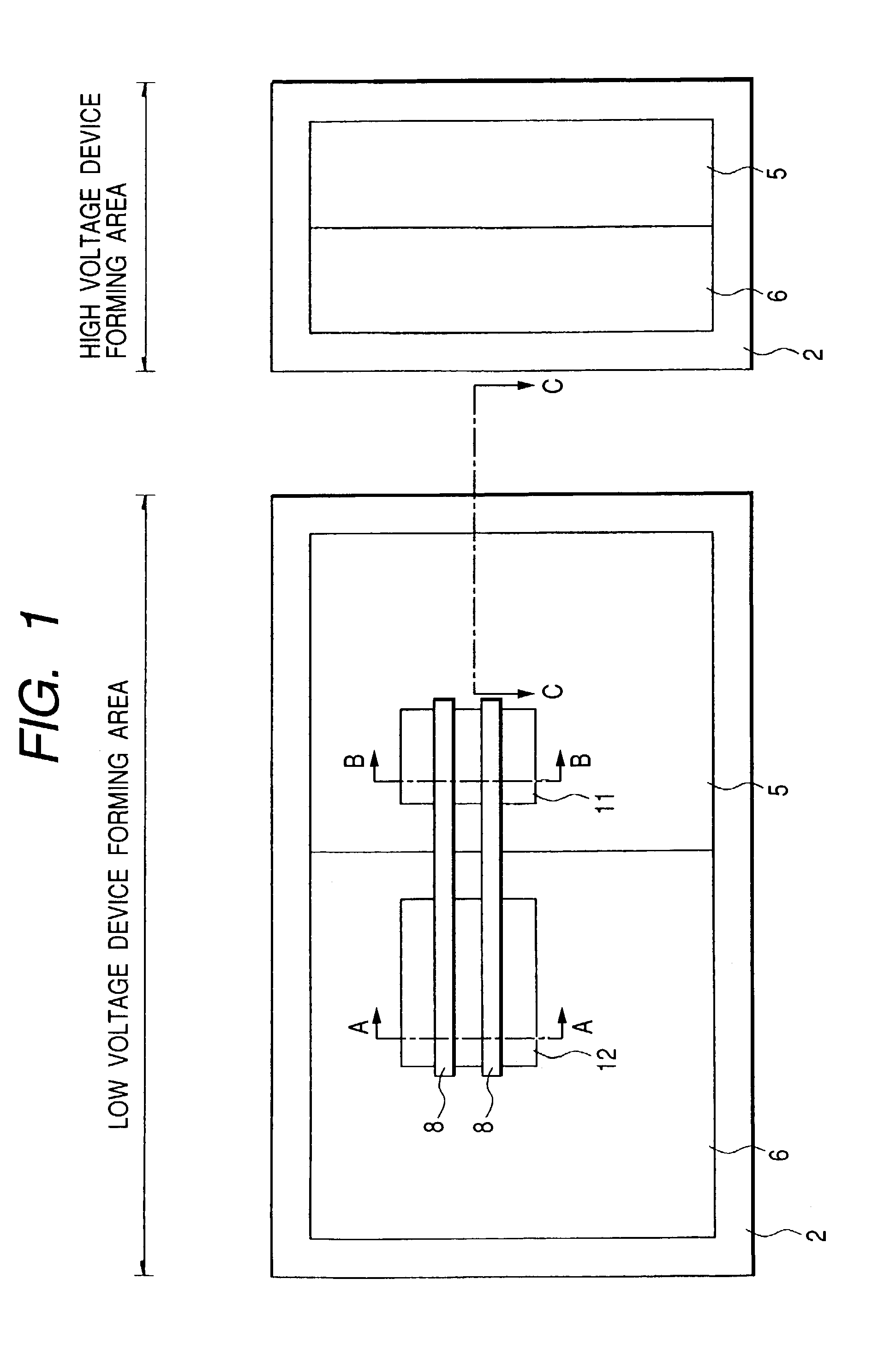
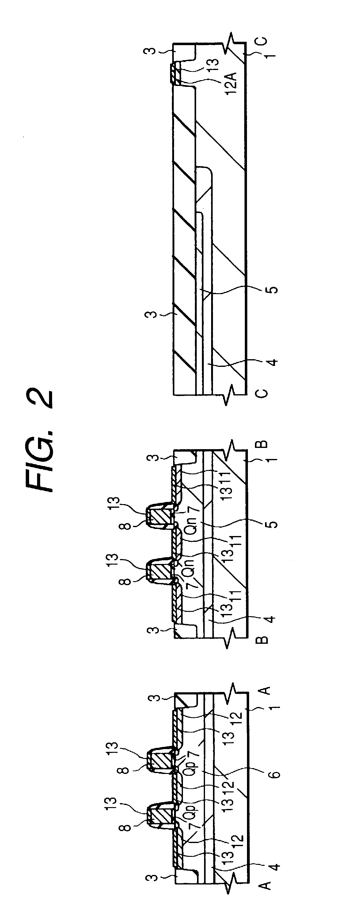
[0132]FIG. 1 is a plan view of a principal portion, illustrating how to fabricate the semiconductor integrated circuit device of the first embodiment and FIG. 2 comprises sectional views taken along lines A—A, B—B and C—C respectively in FIG. 1. In FIG. 1, a low voltage device forming area is an area in which there is formed a circuit with a relatively high voltage applied thereto, while a high voltage device forming area is an area in which there is formed a circuit with a relatively low voltage applied thereto.

[0133]First, as shown in FIGS. 1 and 2, an element isolation region 3 is formed on a semiconductor substrate 1 of a p-type single crystal silicon having a specific resistance o...

second embodiment

[0179]FIG. 34 is a plan view of a principal portion in a manufacturing step for a semiconductor integrated circuit device according to a second embodiment of the present invention and FIG. 35 comprises sectional views taken along lines E—E and F—F respectively in FIG. 34.

[0180]A manufacturing process for the semiconductor integrated circuit device of this second embodiment is about the same as in the previous first embodiment except that there is used a circuit R for correction. In this second embodiment, as shown in FIGS. 34 and 35, a plug (first plug) 43PR and Cu wiring (second buried wiring) 43R are also formed in the step of forming the plug 43P and Cu wiring 43. In this second embodiment, a circuit R for correction is formed beforehand in the semiconductor integrated circuit device. The circuit R is used to correct a circuit connection for example in the event a defect in circuit design should occur in a series of manufacturing steps involving fabrication of the semiconductor i...

third embodiment

[0182]FIG. 37 is a plan view of a principal portion in a manufacturing step for a semiconductor integrated circuit device according to a third embodiment of the present invention.

[0183]A manufacturing process for the semiconductor integrated circuit device of this third embodiment is about the same as the manufacturing process for the semiconductor integrated circuit devices of the first and second embodiments. In this third embodiment, in order to prevent the occurrence of a potential difference between plural Cu wirings 33W as main power lines arranged on the arrangement of cells which form the semiconductor integrated circuit device of this third embodiment and connected electrically to a reference (earth) potential, the plural Cu wirings 33W are connected electrically using Cu wirings 43 which overlie the Cu wirings 33W. That is, the Cu wirings 43 are used as auxiliary power lines for the plural Cu wirings 33W.

[0184]Thus, the Cu wirings 43 used in this third embodiment are auxil...


PUM


Abstract

In a semiconductor integrated circuit device having plural layers of buried wirings, it is intended to prevent the occurrence of a discontinuity caused by stress migration at an interface between a plug connected at a bottom thereof to a buried wiring and the buried wiring. For example, in the case where the width of a first Cu wiring is not smaller than about 0.9 μm and is smaller than about 1.44 μm, and the width of a second Cu wiring and the diameter of a plug are about 0.18 μm, there are arranged two or more plugs which connect the first wirings and the second Cu wirings electrically with each other.

Description

BACKGROUND OF THE INVENTION[0001]The present invention relates to a semiconductor integrated circuit device and a technique for manufacturing the same. Particularly, the invention is concerned with a technique applicable effectively to the fabrication of a semiconductor integrated circuit device having wiring which is formed by burying a conductive film in a wiring-forming groove formed in an insulator.[0002]With improvement in the integration level of elements in a semiconductor integrated circuit device and reduction in size of a semiconductor chip, the wiring which constitutes the semiconductor integrated circuit device is becoming more and more fine and multi-layered. Particularly, in a semiconductor integrated circuit device of a logic type having a multi-layer wiring structure, a wiring delay is one dominant factor of a signal delay in the whole of the semiconductor integrated circuit device. The speed of a signal traveling through the wiring is proportional to both wiring res...

Claims


Application Information

Patent Timeline
Patent Type & Authority Patents(United States)
IPC IPC(8): H01L23/48H01L23/52H01L21/768H01L23/522H01L21/82H01L21/8238H01L23/528H01L23/532
CPCH01L21/823871H01L23/5286H01L23/53238H01L2924/0002H01L2924/00H01L23/5226
Inventor FUNAKOSHI, TAKAKOMURAKAMI, EIICHIYANAGISAWA, KAZUMASATAKEUCHI, KANAOKI, HIDEOYAMAGUCHI, HIZURUOSHIMA, TAKAYUKITSUNOKUNI, KAZUYUKI
Owner RENESAS ELECTRONICS CORP
Why Eureka
Try Eureka