System and method for integrating optical layers in a PCB for inter-board communications

a technology of optical layers and inter-board communication, applied in the field of multi-level printed circuit boards, can solve the problems of increased failure opportunities, slow data transfer rate, and low data rate and increase delay

Inactive Publication Date: 2006-04-04
TTM TECH INC
View PDF12 Cites 8 Cited by
  • Summary
  • Abstract
  • Description
  • Claims
  • Application Information

AI Technical Summary

Benefits of technology

[0013]A further object of the present invention is to develop a method for producing PCBs integrated with optical waveguides using laser technology.
[0014]Yet a further object of the present invention is to develop a method for integrating optical waveguides with a PCB using successive laminations of optical conductive materials of differing refractive indices.

Problems solved by technology

The result is lower data rates and increased delay.
One of the impediments to achieving this objective is the backplane.
Additional cabling may be required to interconnect devices to each other or other points on the backplane resulting in slower data transfer rates, increased opportunities for failure, and increased costs.

Method used


Image

  • System and method for integrating optical layers in a PCB for inter-board communications
  • System and method for integrating optical layers in a PCB for inter-board communications
  • System and method for integrating optical layers in a PCB for inter-board communications

Examples


Embodiment Construction

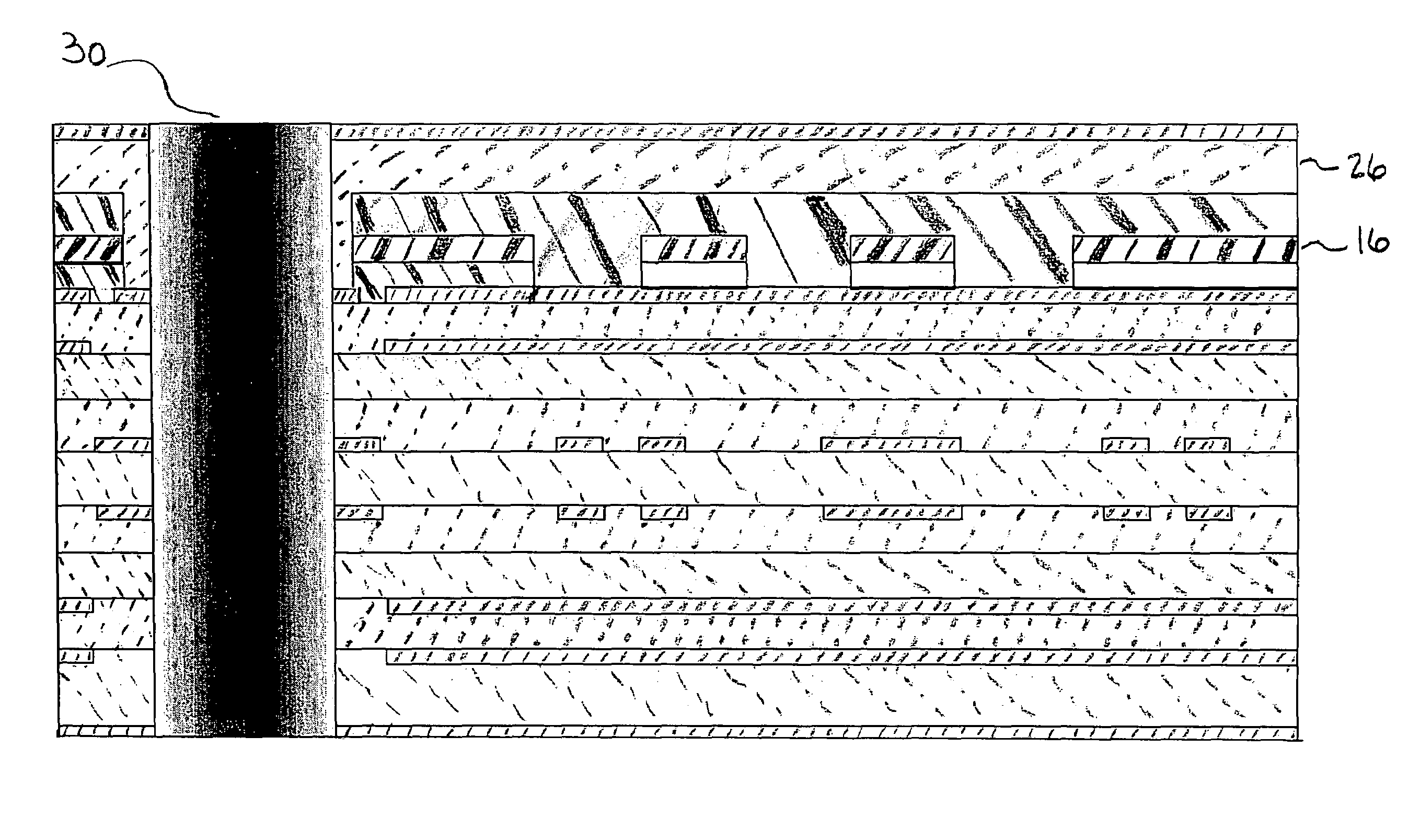
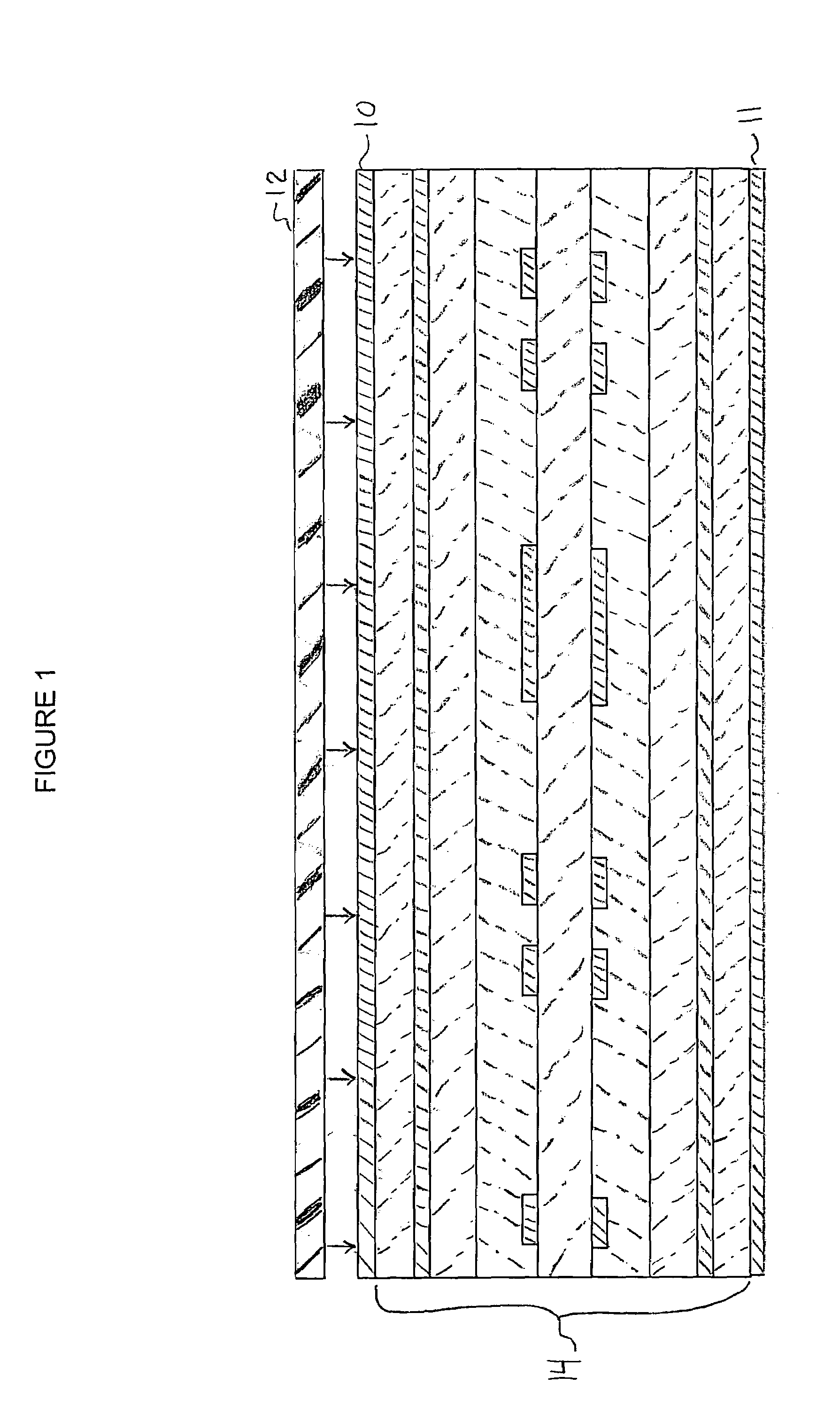
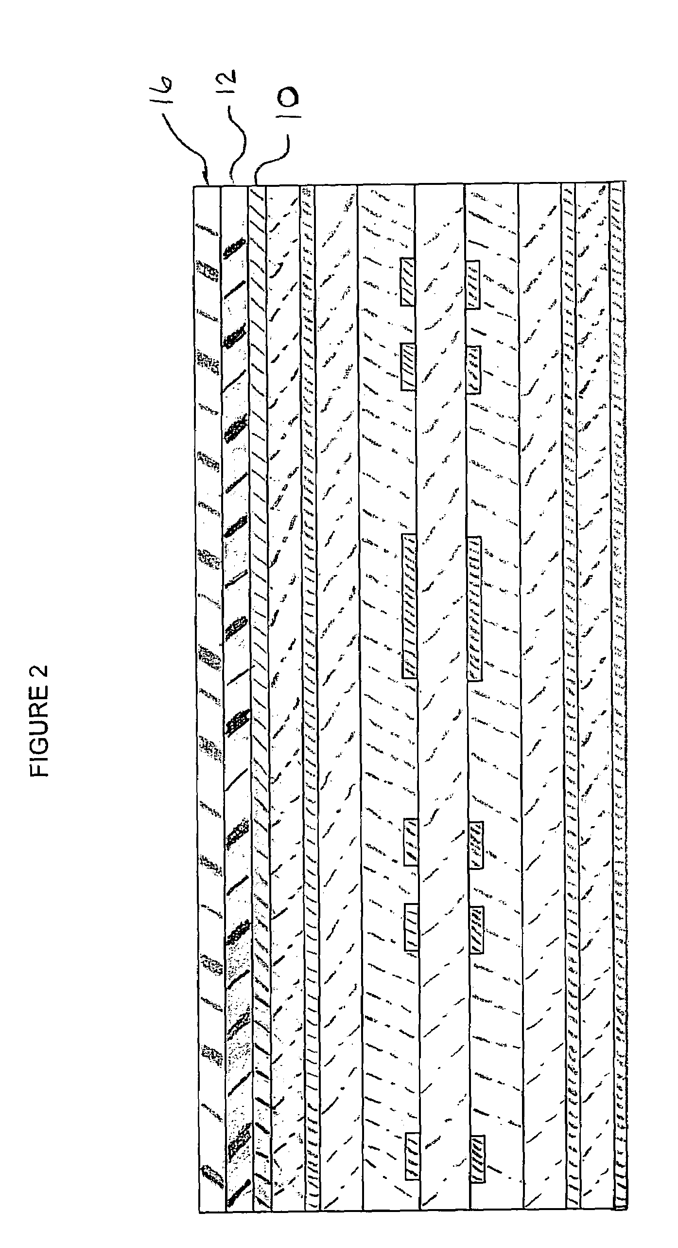
[0030]Referring to FIG. 1, a sectional view is illustrated of a multi-layered PCB with the outer most layers of copper, at an initial stage of optical integration. A multi-layered PCB 14 is covered top and bottom with copper layers 10, 11. In this way, the PCB is first built for supporting electrical circuitry and functions, and then incorporates an optical conductive layer into its structure. The core of the multi-layer PCB is processed before laminating a first optical conductive layer 12. According to one embodiment of the present invention the optical conductive layer 12 is a polymer material sold under the tradename Polyguide™. The first polymer laminate layer 12 has a specific refraction index n2. The laminate covers the entire top surface area of the PCB, over the top copper layer 10.

[0031]According to one embodiment of the present invention, the top copper layer 10 is roughened prior to laminating the surface with the polymer coat 12 in order to improve adhesion. For example...


PUM

PropertyMeasurementUnit
optical transmittingaaaaaaaaaa
refraction indexaaaaaaaaaa
coefficient of thermal expansionaaaaaaaaaa

Abstract

Polymers of differing refraction indices are embedded within a PCB to provide optical connectivity of the PCB with other circuit boards via an optic backplane. The creation of islands of polymer material of refractive index n1 completely surrounded by polymer material with refractive index n2 where n1 has a higher index than n2 allows the islands of n1 indexed polymer to serve as optical waveguides. A process of forming a multi-layered PCB with the optical waveguide islands using successive laminations and using laser ablation to write the optical connection scheme is taught. Further, the use of uniquely marked targets in a copper layer to align the optical waveguides in production is also taught. Additionally, the use of clearing polymer materials and reinforcing polymer voids with lamination to allow a simple, high tolerance insertion of through-holes is taught.

Description

CROSS REFERENCE TO RELATED APPLICATIONS[0001]The present application is a continuation of U.S. Ser. No. 10 / 179,758, filed Jun. 25, 2002, now U.S. Pat. No. 6,834,131, which claims priority under 35 U.S.C. § 119(e) from provisional application no. 60 / 303,380 filed Jul. 6, 2001; the entire contents of which are hereby expressly incorporated herein by reference.BACKGROUND OF THE INVENTION[0002]1. Field of the Invention[0003]The present invention relates generally to the field of printed circuit boards. More particularly, the present invention relates to multi-level printed circuit boards (or “PCBs”) that integrate optical data communications with other boards without electrical connections. That is, the present invention relates to backplane circuit boards that integrate photonic connection.[0004]2. Background Information[0005]Today, much of the world's communication is carried on optical fibers, the data encoded in modulated light. Transmission rates are measured in billions of bits pe...

Claims


Application Information

Patent Timeline
Patent Type & Authority Patents(United States)
IPC IPC(8): G02B6/10C03B37/022G02B6/12G02B6/122G02B6/13G02B6/138G02B6/43H05K1/02H05K3/00H05K3/38H05K3/46
CPCG02B6/138G02B6/43H05K1/0274H05K3/0008H05K2201/09918H05K3/4652H05K2201/0187H05K2201/0195H05K3/0032H05K3/46
Inventor TOURNE, JOSEPH A. A. M.
Owner TTM TECH INC
Why Eureka
Try Eureka