
Method of optimizing signal lines within circuit, optimizing apparatus, recording medium having stored therein optimizing program, and method of designing circuit and recording medium having stored therein program for designing circuit

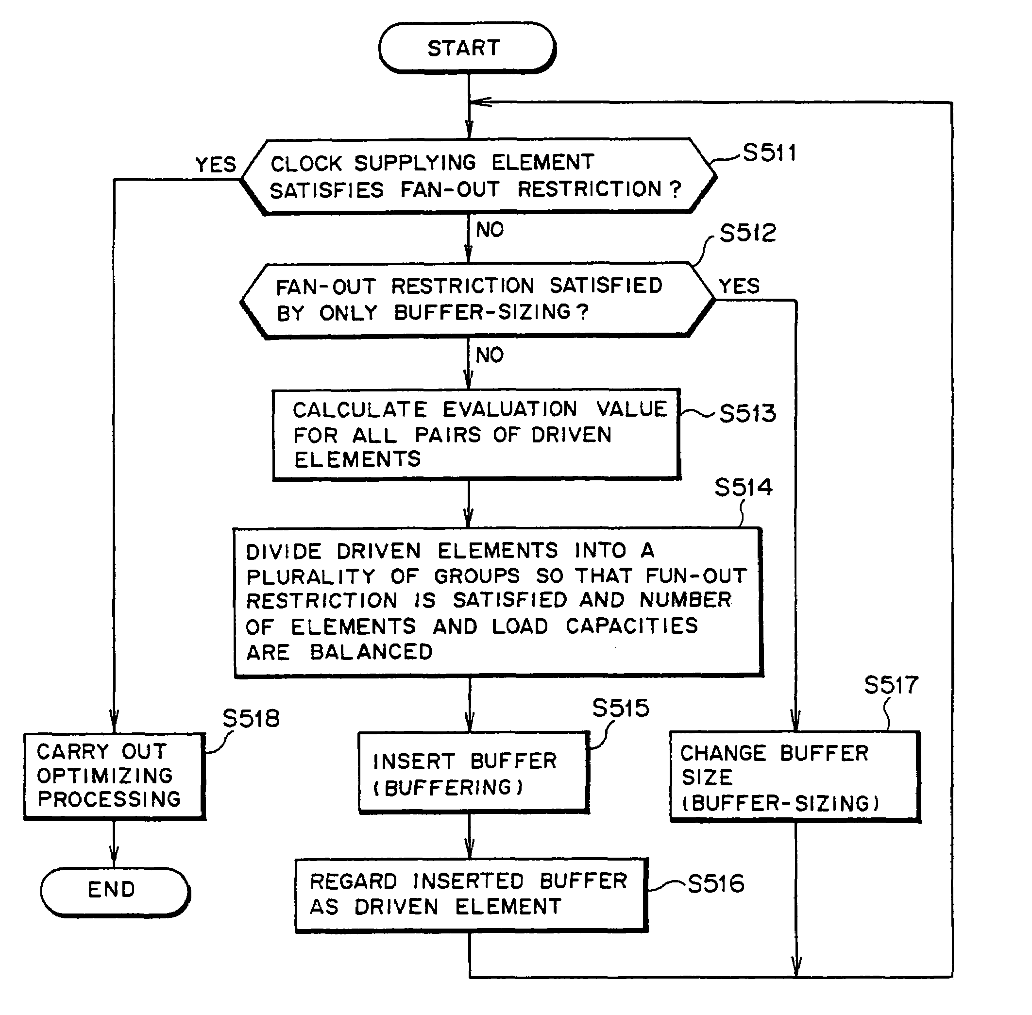
a signal line and circuit technology, applied in the field of optimizing signal lines within circuits, can solve the problems of difficult to adjust the clock skew, complicated fabrication, and difficulty in designing the clock logic of the integrated circuit, and achieve the effect of reducing the probability of timing errors after fixing the layout, reducing the time it takes for the circuit to carry out processing, and efficient arrangemen

Inactive Publication Date: 2006-04-18
SOCIONEXT INC
View PDF21 Cites 20 Cited by
  • Summary
  • Abstract
  • Description
  • Claims
  • Application Information

AI Technical Summary

Benefits of technology

[0072]If the tree-like wired signal lines are created with balance as described above, and thereafter optimization of the signal distribution by the signal lines is effected, then it becomes possible to positively arrange the tree-like wired signal lines causing little skew with ease.
[0094]Further, according to the present invention, even if the circuit under designing contains a locally congested part in wiring, the congested part can be effectively removed, with the result that the entire wiring of the circuit will have a uniform allowance in wiring density. Thus, the circuit having been subjected to the process according to the present invention can be more densely packed and fabricated with a smaller size on a semiconductor chip.

Problems solved by technology

Recently, an integrated circuit such as a VLSI comes to have a great number of circuit components and hence it is fabricated in a complicated fashion owing to the progress of fabrication technology.
With this tendency of technology, a number of elements supplied with a clock signal on the integrated circuit tends to increase, leading to difficulty in designing a clock logic of the integrated circuit.
If scattering in the number of elements or load capacity for every group is large, then scattering of wire length from the final stage buffer element to the driven element in each group also becomes large, with the result that it becomes very difficult to adjust the clock skew.
As a result, there is a fear that a skew adjustment becomes difficult upon arranging layout or that the clock signal line becomes long, which facts lead deterioration in circuit quality.
For this reason, if the clock layout is effected on the logic information so as to satisfy the clock restricting condition, then wiring becomes crowded and clock wiring and signal wiring after the clock wiring will encounter difficulties which prevent the clock wiring and the signal wiring from being carried out.
In this case, signal lines 398 to 401 of a network (hereinafter referred to as net) for driving the floorplan blocks remote from each other become long, with the result that a propagation delay time of the clock signal becomes long and wiring is crowded (first problem).
Such a concentration of the flip-flop placement will cause crowded wiring (second problem).
Further, if the flip-flop cells are moved from initial placement positions to the placement restriction area, then a signal line of the net which is connected to any component other than a flip-flop cell supplied with clock signal may become long, with the result that wiring except for the clock signal also become crowded (third problem). FIG. 64 contains examples of signal lines 441 to 445 which become excessively long.
As a problem other than the problem of crowded wiring, there can be a problem of a skew value of a signal propagation delay time (fifth problem).
In this case, a signal line extending to the flip-flop cell becomes long, and hence the propagation delay time of a signal reaching the cell is increased, with the result that the skew becomes large.
In this case, a clock path including two stages of buffer and a clock path including three stages of buffer will have signal propagation delay times different from each other, with the result that the sew becomes large (sixth problem).
Therefore, wiring paths of data path 359 connecting the flip-flop cells to one another intersects one another, resulting in complicated wiring.
In addition, a data path 459, and clock paths 457 and 458 become long, which causes a timing error (seventh problem).
The above-introduced first problem derives from a fact that the layout information is not taken into account when the clock tree is created.
The above-introduced second and third problems derive from facts that the placement restriction areas can be overlaid on one another, and driven cells are forcibly moved into the overlapped portion of the placement restriction areas when the placement is retried.
The above-introduced fourth problem derives from a fact that a wiring between a buffer cell for driving another cell and buffer cells which are driven by that buffer cell is arranged merely as a radiated fashion.
The above-introduced fifth problem derives from a fact that the conventional method employs a scheme that flip-flop cells are merely subjected to a placement retry within the placement restricted area.
The above-introduced sixth problem derives from a fact that if the clock tree includes modules having different buffer stages, then a clock skew causing in the path becomes large.
The above-introduced seventh problem derives from a fact that flip-flop cells are placed upon initial placement with a clock path not disregarded.

Method used


Image

  • Method of optimizing signal lines within circuit, optimizing apparatus, recording medium having stored therein optimizing program, and method of designing circuit and recording medium having stored therein program for designing circuit
  • Method of optimizing signal lines within circuit, optimizing apparatus, recording medium having stored therein optimizing program, and method of designing circuit and recording medium having stored therein program for designing circuit
  • Method of optimizing signal lines within circuit, optimizing apparatus, recording medium having stored therein optimizing program, and method of designing circuit and recording medium having stored therein program for designing circuit

Examples


first embodiment

[0161][1] Description of a

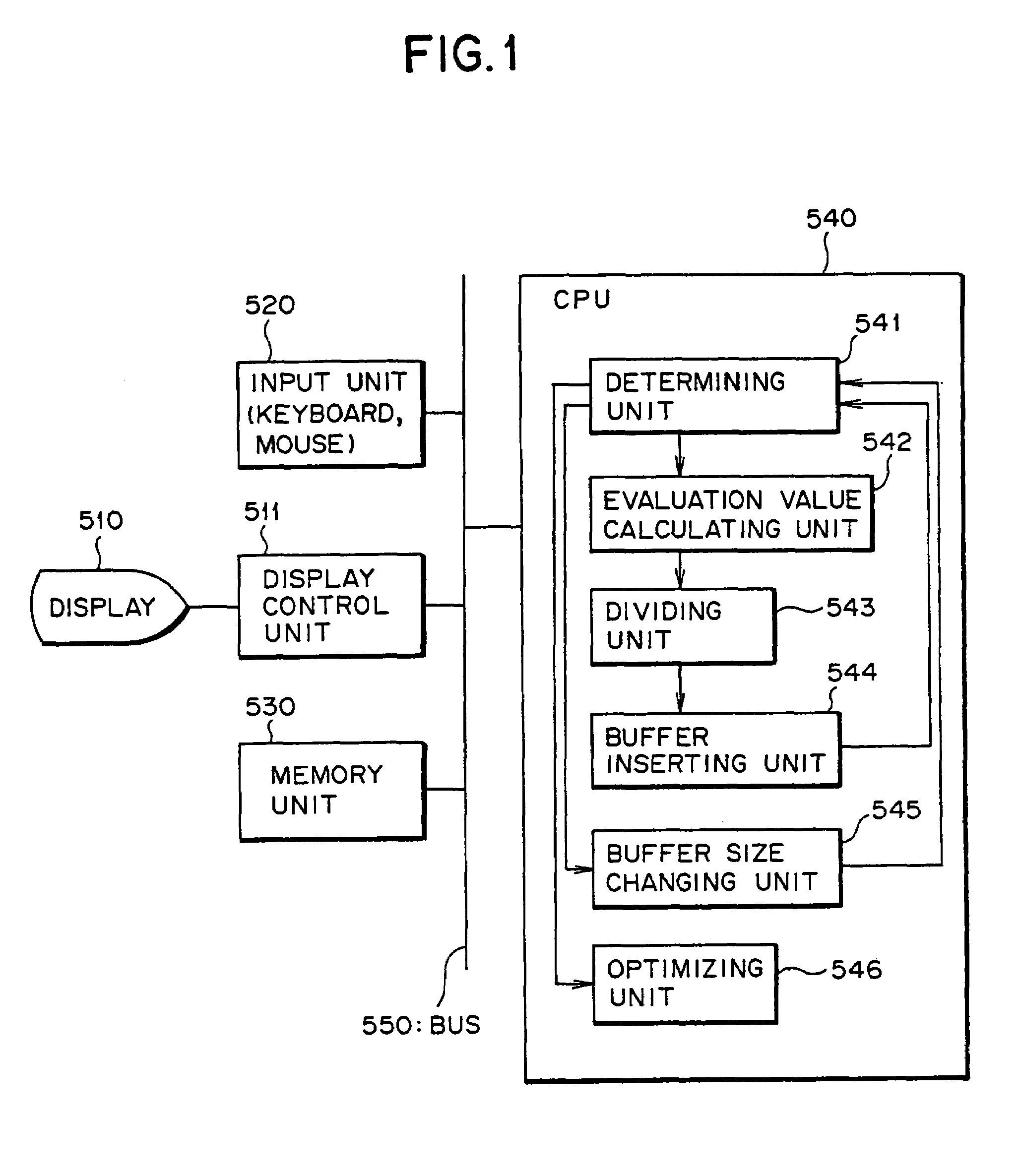
[0162]FIG. 1 is a block diagram showing a functional arrangement of an optimizing apparatus for optimizing signal lines within a circuit as a first embodiment of the present invention. The optimizing apparatus shown in FIG. 1 is utilized when a designer designs a circuit (e.g., a VLSI) including a clock supplying element (clock supplying source) and a number of elements (driven elements; in this case, flip-flops) supplied with a signal from the clock supplying element. When the above-described circuit is designed, the optimizing apparatus optimizes signal distribution through clock signal lines (clock system net) connecting the clock supplying element to the number of FFs in terms of clock distribution. Thus, as shown in FIG. 1, the optimizing apparatus is arranged to include a display 510, a display control unit 511, an input unit 520, a memory unit 530, a general processing unit (processor, computer) having a CPU 540 or the like.

[0163]According to the abo...

second embodiment

[0234][2] Description of a Second Embodiment

[0235]FIG. 15 is a block diagram showing a functional arrangement of an optimizing apparatus for optimizing signal lines within a circuit as a second embodiment of the present invention. As shown in FIG. 15, the optimizing apparatus of the second embodiment is similarly arranged to the apparatus of the first embodiment shown in FIG. 1. However, the arrangement of the second embodiment includes the CPU 540 added with a function as a buffer stage number adjusting unit 47.

[0236]The buffer stage number adjusting unit 547 serves as a function unit that inserts one ore more buffer elements 503 into paths extending from the clock supplying element 501 to each of the FFs 502 so that the number of cell stages become equal among the all paths extending from the clock supplying element 501 to the FFs 502. In this case, the cells include, in addition to the buffer element 503, a logic gate or a selector to be incorporated into the clock system net.

[02...

third embodiment

[0243][3] Description of a

[0244]FIG. 18 is a block diagram showing a functional arrangement of an optimizing apparatus for optimizing signal lines within a circuit as a third embodiment of the present invention. As shown in FIG. 18, the optimizing apparatus of the third embodiment also is arranged similarly to the apparatus of the first embodiment shown in FIG. 1. However, the arrangement of the third embodiment is additionally provided with an insert buffer estimating unit 548 and an insert buffer selecting unit 549 at the CPU 540.

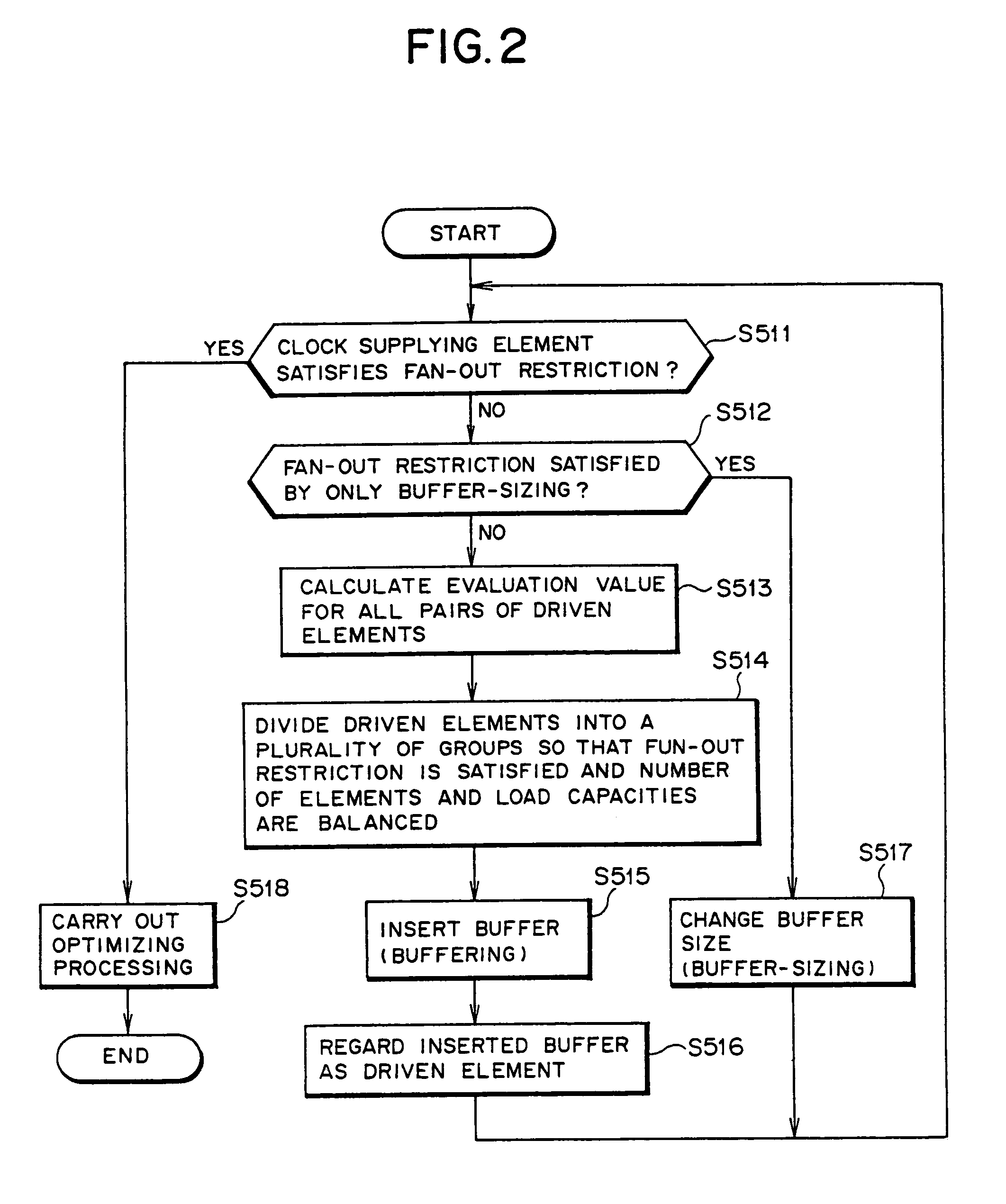
[0245]When the determining unit 541 determines that the clock tree arrangement of the current status does not satisfy a fan-out restriction and buffer-sizing operation is insufficient for making the clock tree satisfy the fan-out restriction, then the insert buffer estimating unit 548 estimates the number of stages of buffer elements that are to be inserted into the clock tree based on a load capacity and a number of driven elements of the clock tree.

[024...


PUM


Abstract

A method for designing an integrated circuit such as a VLSI circuit, in particular optimizing delay of a signal transmitting through signal lines connecting a signal supplying source to each of elements, whereby skew can be decreased. The method can include determining whether the signal source satisfies a fan-out restriction if the signal source supplies a signal to all of the driven elements which are directly connected to the signal source, dividing the elements into groups so that the fan-out restriction is satisfied in each of the groups and each of the groups has the same or substantially same load capacity, when the signal source does not satisfy the fan-out restriction, and inserting into each group, a buffer having a size which makes the groups of elements satisfy the fan-out restriction. The dividing and the buffer inserting are repeated until a positive determination is delivered on the fan-out restriction.

Description

[0001]This is a DIV of 09 / 600,144 filed Jul. 12, 2000 now U.S. Pat. No. 6,651,224 which is a 371 of PCT / JP99 / 00205 filed Jan. 21, 1999.TECHNICAL FIELD[0002]The present invention relates to a technology utilized when designing a circuit which includes a signal supplying source (e.g., clock signal supplying source) within the circuit and a plurality of elements (e.g., flip-flop cells) supplied with a signal from the signal supplying source.[0003]In more particularly, the present invention relates to a method of optimizing signal lines within the circuit, an optimizing apparatus and a recording medium having stored therein an optimizing program which are utilized when automatically synthesizing signal lines (net) connecting the signal supplying source to each of the elements in which a buffering scheme of a clock system net (signal lines) on an integrated circuit such as a VLSI is improved so that a delay or a skew of a signal from the signal supplying source to each of the elements is...

Claims


Application Information

Patent Timeline
Patent Type & Authority Patents(United States)
IPC IPC(8): G06F17/50G06F9/45
CPCG06F17/505G06F30/327
Inventor SANO, MASAHIROSUGIOKA, TOSHIAKI
Owner SOCIONEXT INC
Learn More