Method of manufacturing high Q on-chip inductor

a high-q, on-chip technology, applied in the direction of magnets, cores/yokes, magnets, etc., can solve the problems of limiting the usefulness of applications and reducing the sensitivity of receivers

Inactive Publication Date: 2006-04-25
AVAGO TECH INT SALES PTE LTD
View PDF4 Cites 6 Cited by
  • Summary
  • Abstract
  • Description
  • Claims
  • Application Information

AI Technical Summary

Benefits of technology

[0009]The high Q on-chip inductor of the present invention substantially meats these needs and others. In general, the high Q on-chip inductor includes a primary winding and an auxiliary winding that is coupled to receive a proportionally opposite representation of an input of the primary winding (i.e., reversed biased). Further, the auxiliary winding has a real part of its admittance greater than the real part of the admittance of the primary winding thereby yielding an asymmetry in the admittances. As such, a push / pull mechanism is obtained in a 2-port system (e.g., 1st and 2nd nodes of the primary winding) that produces a large Q factor (e.g., at least 30) for an on-chip inductor.
[0011]A further embodiment includes a primary winding, a primary auxiliary winding, a secondary winding, and a secondary auxiliary winding thus producing a high quality factor on-chip transformer. The secondary auxiliary winding is coupled to receive a proportionally opposite representation of the signal of the secondary winding. Further, the secondary auxiliary winding has a real part of its admittance greater than the real part of the admittance of the secondary winding thereby yielding an asymmetry in the admittances.

Problems solved by technology

In addition, high Q inductors minimize the power leaking into adjacent channels that corrupts a receiver performance in nearby channels of communication chips, which degrade a receiver's sensitivity.
While performance of wireless communication devices is a critical design issue it is typically balanced with manufacturing costs of the devices.
However, on-chip inductors using CMOS technology are known to have a modest quality factor in the range of 5 to 10, which limit their usefulness is applications that require a high Q inductor, including some wireless communication applications.

Method used


Image

  • Method of manufacturing high Q on-chip inductor
  • Method of manufacturing high Q on-chip inductor
  • Method of manufacturing high Q on-chip inductor

Examples


Embodiment Construction

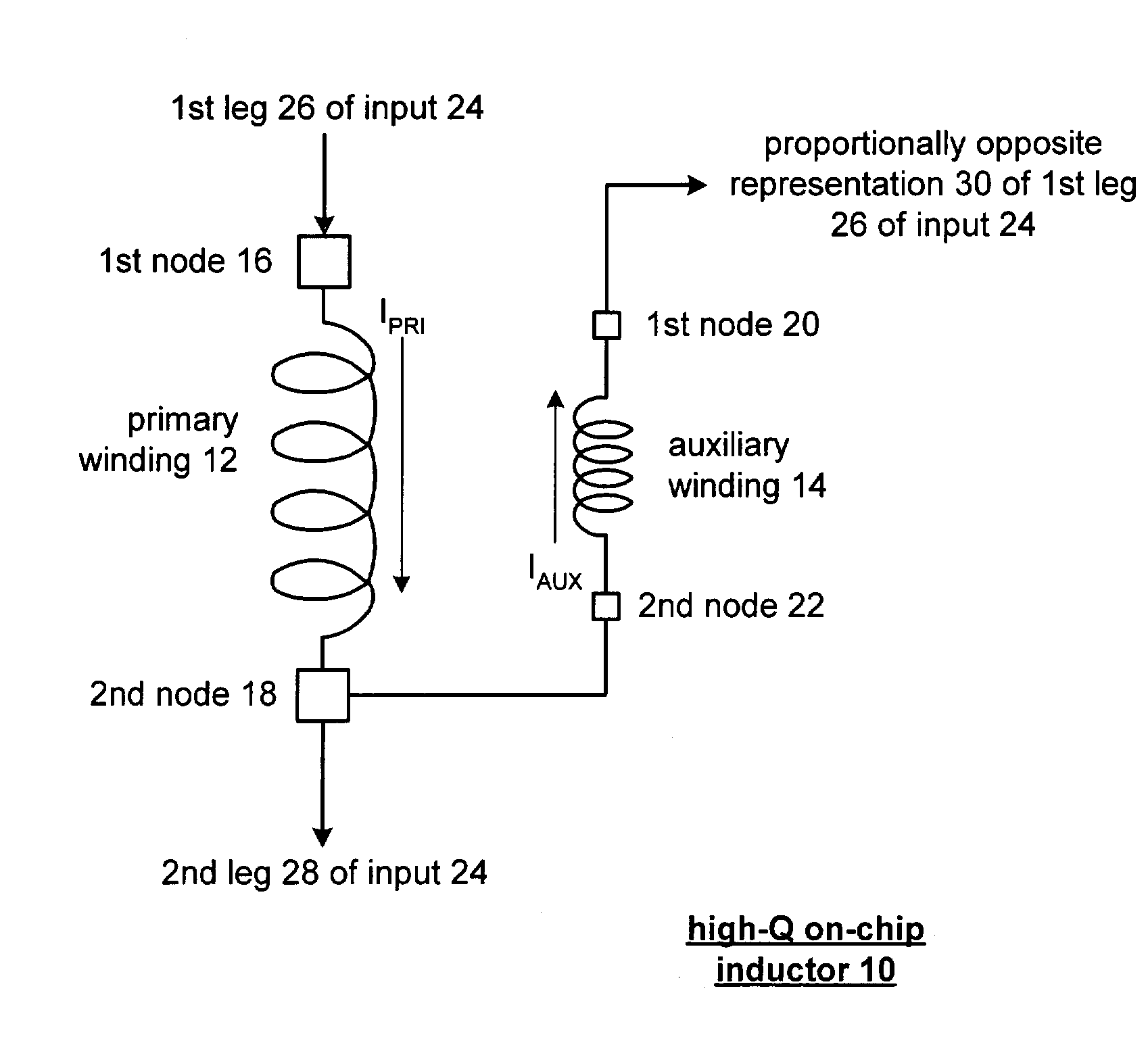
[0020]FIG. 1 illustrates a schematic block diagram of a high Q (i.e., quality factor) on-chip inductor 10 that includes a primary winding 12 and an auxiliary winding 14, which may be fabricated using CMOS technology, gallium arsenide technology, silicon germanium technology, or any other type of integrated circuit technology. The primary winding 12 includes a 1st node 16 and a 2nd node 18. The auxiliary winding 14 includes a 1st node 20 and a 2nd node 22. As shown, the 2nd node 18 of primary winding 12 is coupled to the 2nd node 22 of the auxiliary winding 14. The 1st node 16 and 2nd node 18 of primary winding 12 are operably coupled to receive a 1st leg 26 and 2nd leg 28 of an input 24, respectively. As such, a current (IPRI) flows through the primary winding 12 based on the magnitude of the input 24 imposed across the 1st node 16 and 2nd node 18 and the inductance value of the primary winding. As one of average skill in the art will appreciate, the input 24 may be a voltage input ...


PUM

PropertyMeasurementUnit
operating frequencyaaaaaaaaaa
admittanceaaaaaaaaaa
admittancesaaaaaaaaaa

Abstract

A high Q on-chip inductor includes a primary winding and an auxiliary winding that is coupled to receive a proportionally opposite representation of an input of the primary winding. Further, the auxiliary winding has an admittance that is greater than the admittance of the primary winding thereby yielding an asymmetry in the admittances. As such, a push / pull mechanism is obtained in a 2-port system (e.g., 1st and 2nd nodes of the primary winding) that produces a large Q factor for an on-chip inductor.

Description

[0001]This patent application is a DIVISION and is claiming priority under 35 USC §121 to a patent application entitled HIGH Q ON-CHIP INDUCTOR AND METHOD OF MANUFACTURE THEREOF, having a of Ser. No. 10 / 087,614 and a filing date of Mar. 1, 2002 U.S. Pat. No. 6,809,623.TECHNICAL FIELD OF THE INVENTION[0002]This invention relates generally to integrated circuits and more particularly to on-chip inductors.BACKGROUND OF THE INVENTION[0003]As is known, wireless communications standards place stringent requirements on a wireless communication device's dynamic range of operation because the signal strength of received signals may vary by many orders of magnitude. To meet these requirements, wireless communication devices are designed using radio frequency (RF) integrated circuits (IC) that consume low power and produce little noise. As is also known, on-chip inductors are significant components of RF integrated circuits and are used in oscillators, impedance matching networks, emitter dege...

Claims


Application Information

Patent Timeline
Patent Type & Authority Patents(United States)
IPC IPC(8): H01F7/06H01C10/06H01F5/00H01F17/00H01L27/08
CPCH01F17/0006H01L27/08H01F17/0013Y10T29/49071Y10T29/4902Y10T29/49069Y10T29/49073Y10T29/49082Y10T29/4914
Inventor KYRIAZIDOU, SISSYCONTOPANAGOS, HARRYROFOUGARAN, REZA
Owner AVAGO TECH INT SALES PTE LTD
Why Eureka
Try Eureka