Method of making a long wavelength indium gallium arsenide nitride (InGaAsN) active region

a technology of indium gallium arsenide nitride and active region, which is applied in the direction of crystal growth process, polycrystalline material growth, semiconductor lasers, etc., can solve the problems of long growth time, inability to scale well, and inability to produce high-volume light-emitting devices, etc., to maximize the concentration of nitrogen precursors, minimize concentration, excellent electro-optical properties

Inactive Publication Date: 2006-04-25
AVAGO TECH WIRELESS IP SINGAPORE PTE
View PDF9 Cites 4 Cited by
  • Summary
  • Abstract
  • Description
  • Claims
  • Application Information

AI Technical Summary

Benefits of technology

[0014]The invention provides in a fourth aspect a method of making the active region of a long-wavelength light emitting device. In the method, an organometallic vapor phase epitaxy (OMVPE) reactor is provided and a substrate wafer is placed in the reactor. A Group III precursor mixture and a Group V precursor mixture are supplied to the reactor. The Group V precursor mixture comprises a gallium precursor and an indium precursor. The Group V precursor mixture comprises an arsenic precursor and a nitrogen precursor. A layer of indium gallium arsenide nitride having a nitrogen fraction commensurate with light emission at a wavelength longer than 1.2 μm is grown over the substrate wafer. The growing comprises minimizing the concentration of the arsenic precursor consistent with growth of material of high electro-optical quality and maximizing the concentration of the nitrogen precursor in the Group V precursor mixture.
[0015]Embodiments of the invention enable the growth of epitaxial layers of InGaAsN having excellent electro-optical properties and a nitrogen fraction in a design range from about 0.2% to about 5%. Such layers can be used to generate light at wavelengths longer than about 1.2 μm.

Problems solved by technology

However, MBE suffers from a low growth rate, resulting in a long growth time.
Moreover, MBE does not scale well, and therefore does not lend itself to high-volume production of light emitting devices.
High quality films of InGaAsN are difficult to grow using OMVPE because the purity of the nitrogen precursor is difficult to control.
These factors cause the distribution of nitrogen in the layer to be non-uniform.
This results in bandgap fluctuations throughout the layer.
Furthermore, DMHy does not readily decompose to yield atomic nitrogen.
This makes it difficult to grow InGaAsN with a nitrogen fraction sufficient to reduce the band gap of the material to one corresponding to emission at 1.3 μm.
However, reducing the flow of the arsenic precursor tends to reduce the optical quality of the InGaAsN film.
The presence of indium in the grown material makes the incorporation of nitrogen even more problematic.
Nevertheless, a nitrogen content of even 1% is difficult to attain using conventional OMVPE, even when the nitrogen precursor exceeds 90% of the total Group V precursors.

Method used


Image

  • Method of making a long wavelength indium gallium arsenide nitride (InGaAsN) active region
  • Method of making a long wavelength indium gallium arsenide nitride (InGaAsN) active region
  • Method of making a long wavelength indium gallium arsenide nitride (InGaAsN) active region

Examples


first embodiment

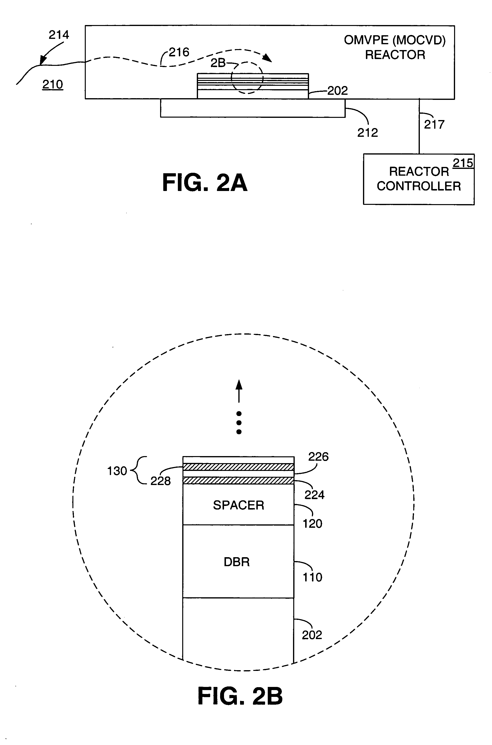
[0043]FIG. 2B is a detailed view of VCSEL 100 shown in FIG. 2A part-way through the process of growing the layer structure. The epitaxial layers that form DBR 110 and lower cavity spacer layer 120 have been deposited on substrate wafer 202 by OMVPE at a conventional growth pressure, which is less than or equal to 100 mbar. After deposition of these layers, and in accordance with the invention, the growth pressure in OMVPE reactor 210 is increased to a sub-atmospheric elevated growth pressure and active region 130 is then grown on lower cavity spacer layer 120. Increasing the growth pressure in the OMVPE reactor to a sub-atmospheric elevated growth pressure allows the InGaAsN quantum well layers to be grown with good electro-optical properties but with the flow rate of the arsenic precursor reduced relative to that used at a conventional growth pressure. The lower flow rate of the arsenic precursor increases the effective concentration of the nitrogen precursor in the flow of precurs...

second embodiment

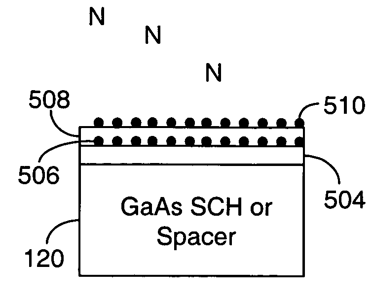
[0070]FIGS. 6A through 6F are schematic views illustrating a method in accordance with the invention for epitaxially growing a quantum well layer of InGaAsN having a high nitrogen fraction. The quantum well layer is shown being grown on the surface of lower cavity spacer layer 120. DBR 110 (FIG. 1A) and lower cavity spacer layer 120 are grown on a substrate wafer 202 (FIG. 2A) as described above with reference to FIG. 2A. In FIG. 6A, an indium precursor, a gallium precursor, an arsenic precursor and a carrier gas have been supplied to an OMVPE reactor similar to that shown in FIG. 2A to grow a sublayer 504 on the surface of lower cavity spacer layer 120. The material of the sublayer is InGaAs and the sublayer has a thickness of one or two atoms.

[0071]In FIG. 6B, a growth stop is performed. In the growth stop, the flow of the Group III precursors is discontinued. Additionally, the arsine flow rate is lowered and a high flow rate of a nitrogen precursor supplied to the reactor. This e...


PUM

PropertyMeasurementUnit
internal quantum efficiencyaaaaaaaaaa
partial pressureaaaaaaaaaa
pressureaaaaaaaaaa

Abstract

The active region of a long-wavelength light emitting device is made by providing an organometallic vapor phase epitaxy (OMVPE) reactor, placing a substrate wafer capable of supporting growth of indium gallium arsenide nitride in the reactor, supplying a Group III–V precursor mixture comprising an arsenic precursor, a nitrogen precursor, a gallium precursor, an indium precursor and a carrier gas to the reactor and pressurizing the reactor to a sub-atmospheric elevated growth pressure no higher than that at which a layer of indium gallium arsenide layer having a nitrogen fraction commensurate with light emission at a wavelength longer than 1.2 μm is deposited over the substrate wafer.

Description

RELATED APPLICATION[0001]This application is a Continuation-in-Part of U.S. patent application Ser. No. 10 / 140,625 filed May 7, 2002 now U.S. Pat. No. 6,756,325, of David P. Bour et al. entitled Method Of Producing A Long Wavelength Indium Gallium Arsenide Nitride (InGaAsN) Active Region filed on 7 May 2002, the disclosure of which is incorporated into this application by reference.BACKGROUND[0002]Light emitting devices are used in many applications including optical communication systems. Optical communication systems continue to increase in use due to the large bandwidth they provide for transporting information signals such as voice and data signals. Optical communication systems provide a broad bandwidth and high speed and are suitable for efficiently communicating information signals at high data rates over long distances. Over long distances, optical communication systems operate at relatively long wavelengths, in the order of 1.3 micrometers (μm) to 1.55 μm, because optical f...

Claims


Application Information

Patent Timeline
Patent Type & Authority Patents(United States)
IPC IPC(8): H01L21/44C30B25/02H01L21/205H01L33/00H01L33/10H01S5/323H01S5/343
CPCC30B25/02C30B29/403H01L21/02395H01L21/02507H01L21/0254H01L21/02546H01L21/0262H01L21/02463H01L33/007H01L33/105H01S5/32366Y10S438/956Y10S438/936Y10S438/938
Inventor BOUR, DAVID P.TAKEUCHI, TETSUYATANDON, ASHISHCHANG, YING-LANTAN, MICHAEL R. T.CORZINE, SCOTT W.
Owner AVAGO TECH WIRELESS IP SINGAPORE PTE
Why Eureka
Try Eureka