Long working distance incoherent interference microscope

a long working distance, interference microscope technology, applied in the field of microscopy and metrology, can solve the problems of device malfunction, cross-wafer non-uniformity, residual stress, stress gradient, etc., and achieve excellent image quality, reduced overall system cost, cost and time, and high fringe contrast

Active Publication Date: 2006-04-25
NAT TECH & ENG SOLUTIONS OF SANDIA LLC
View PDF11 Cites 54 Cited by
  • Summary
  • Abstract
  • Description
  • Claims
  • Application Information

AI Technical Summary

Benefits of technology

[0032]The present invention relates to full-field imaging, long working distance, incoherent interference microscope suitable for three-dimensional imaging and metrology of MEMS devices and test structures on a standard microelectronics probe station. A long working distance of 10–30 mm allows standard probes or probe cards to be used. This enables nanometer-scale 3-dimensional height profiles of MEMS test structures to be acquired across an entire wafer while being actively probed, and, optionally, through a transparent window. An optically identical pair of sample and reference arm objectives is not required, which reduces the overall system cost, and also the cost and time required to change sample magnifications. Using a LED source, high magnification (e.g., 50×) can be obtained having excellent image quality, straight fringes, and high fringe contrast.

Problems solved by technology

The microstructure of the resulting films and structures can exhibit cross-wafer non-uniformities, resulting in variations of thickness, height, residual stress, stress gradient, or elastic modulus across the wafer.
Also, highly curved comb drive fingers or suspensions (caused by stress gradient) will result in device malfunction.
Furthermore, surface properties such as adhesion and friction are very sensitive to processing, and may exhibit cross-wafer non-uniformity as well.
Poor quality control of surface properties may result in failure of devices that rely on contact or sliding of surfaces.
However, because of electron charging and calibration problems, it is difficult to obtain the required nanometer scale resolution by this technique.
Other metrology techniques, such as AFM (Atomic Force Microscope) and contact profilometry, can provide the required nanometer-scale resolution to accurately measure 3-D out-of-plane features of IC's and MEMS devices, but either require extensive sample preparation, or rely on potentially destructive contact with the sample surface.
Other non-contact techniques, such as conventional light microscopy, do not provide the required nanometer-scale resolution.
However, this system does not provide nanometer-scale measurement of the surface topography of the MEMS structures.
This arrangement unfortunately reduces the available free working distance to less than 10 mm (especially at higher magnifications, e.g., 20–50×).
Additionally, in this configuration interference fringes cannot be easily obtained through a transparent window (such as might be found in a vacuum chamber) due to the phase shift induced by the window.
Normal manufacturing tolerances do not guarantee that any two objectives intended to be the same (i.e. having the same design and manufacturing specifications) are sufficiently identical for use in a Linnik interferometer.
It is difficult, time-consuming, and, hence, expensive to obtain two optically identical long working distance (LWD) sample objectives, especially at high magnification (e.g., 50×).
In addition, changing the overall magnification of the microscope (e.g., from 5× to 20×) requires that both of the optically identical objectives be changed at the same time, and replaced with another pair of (different power) optically identical objectives, which adds additional time and expensive.
So, having a system with, for example, four different magnifications (e.g., 5×, 10×, 20×, and 50×) would require four pairs of optically identical objectives, for a total of eight objectives, which becomes quite expensive.

Method used


Image

  • Long working distance incoherent interference microscope
  • Long working distance incoherent interference microscope
  • Long working distance incoherent interference microscope

Examples


Embodiment Construction

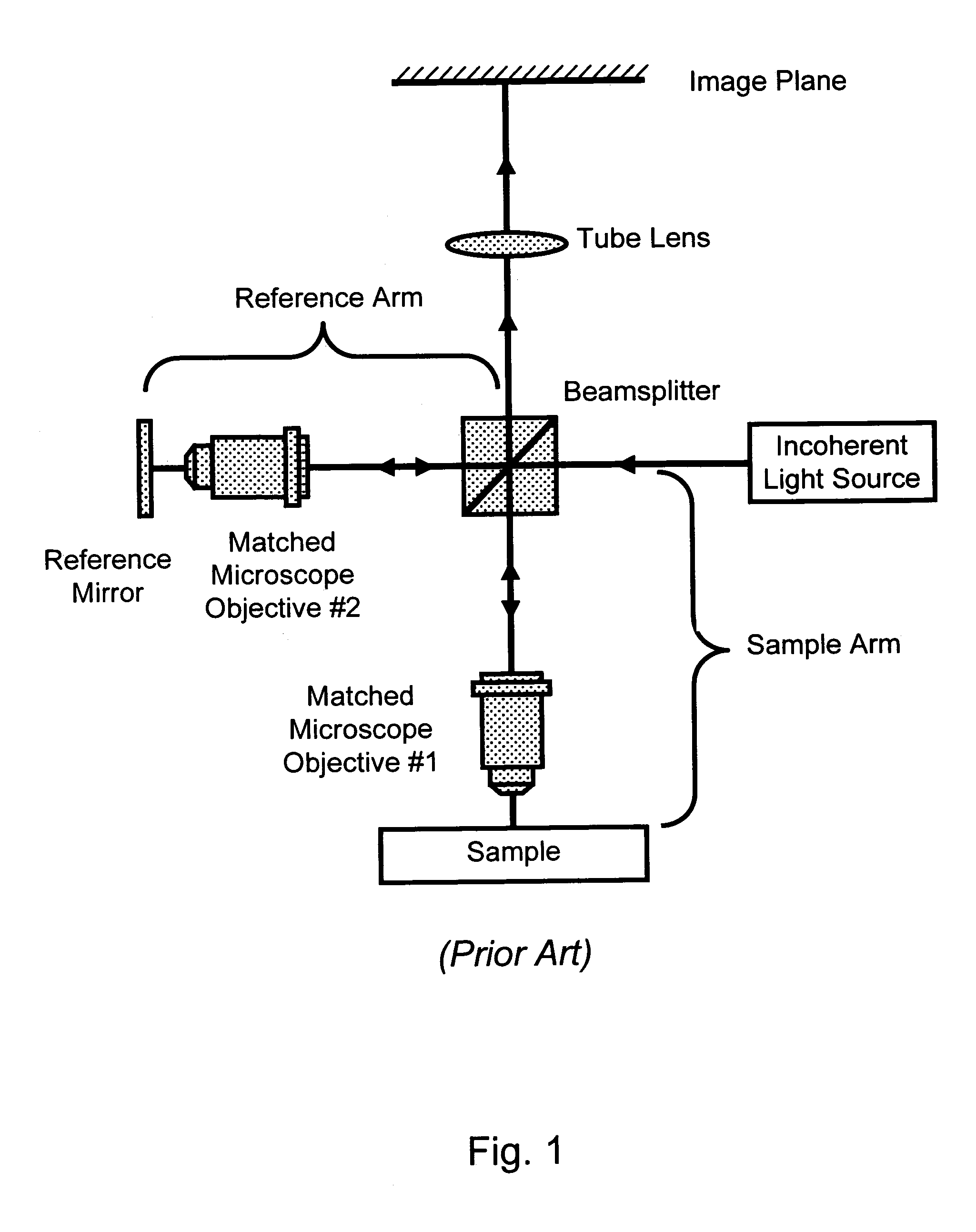
[0033]FIG. 1 (prior art) illustrates a schematic layout of a well-known Linnik microinterferometer, which is based on a two-beam Michelson interferometer. The Linnik microinterferometer requires a pair of optically identical sample and reference objectives when operated with an incoherent light source, such as a LED.

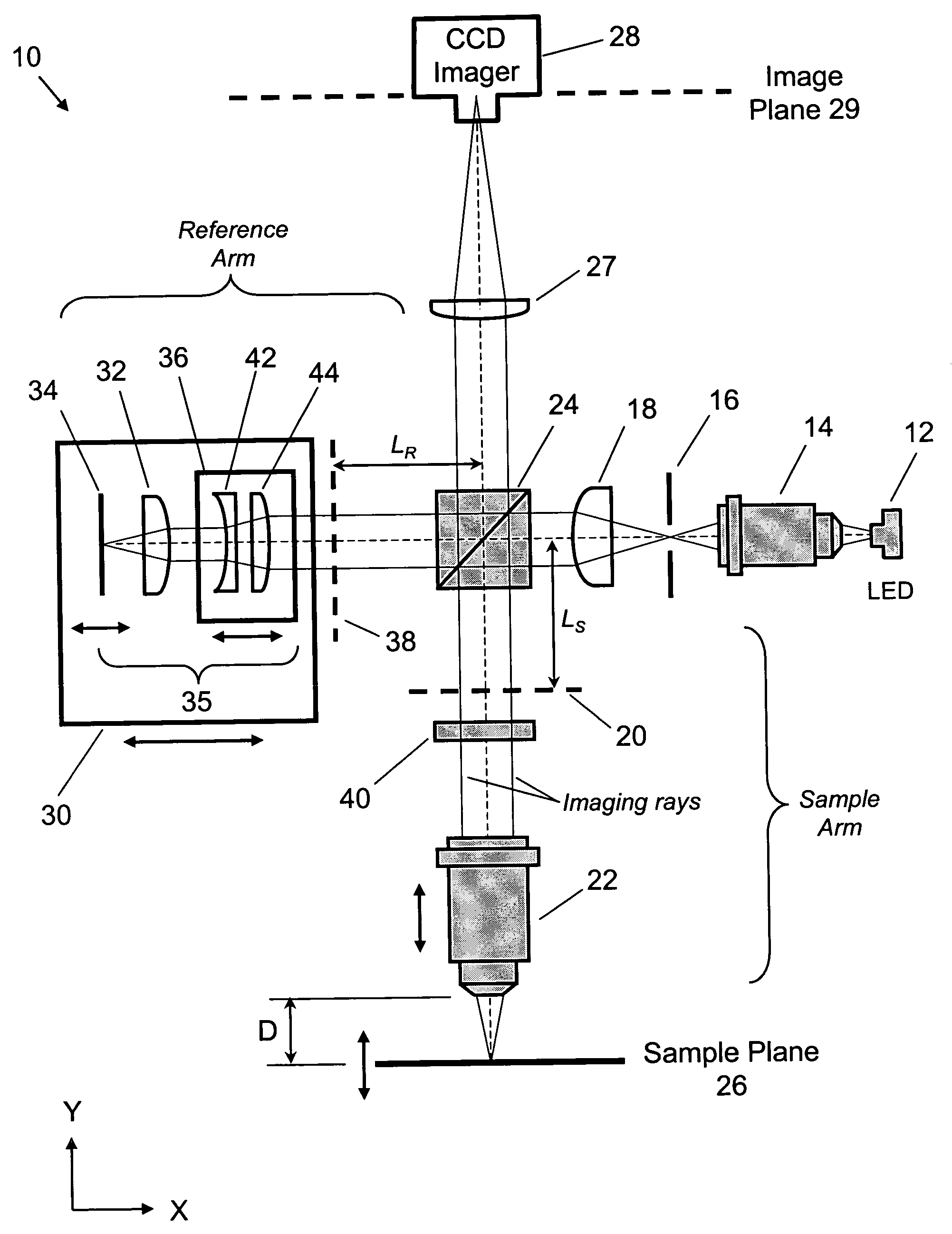
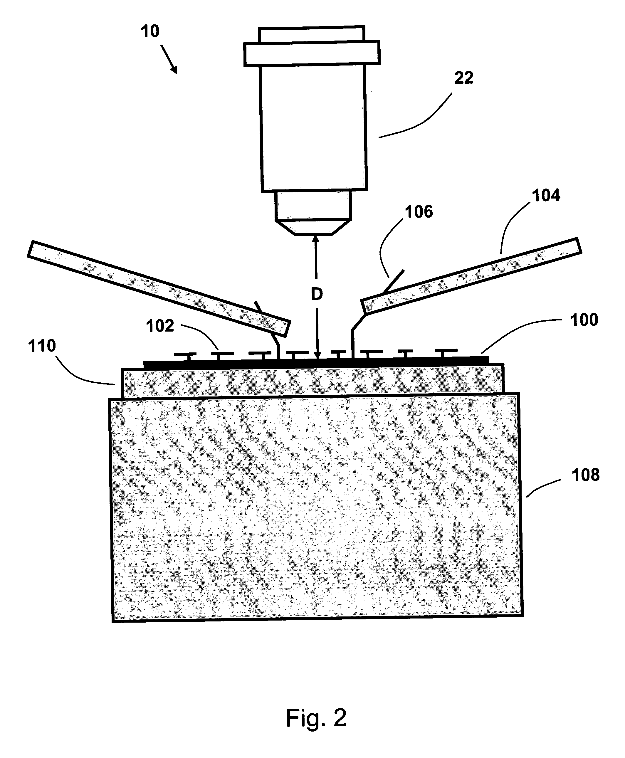
[0034]FIG. 2 illustrates a schematic side view of a first example of a long working distance incoherent interference microscope 10, according to the present invention. Microscope 10 has a long working distance (LWD) sample objective 22, with its tip located at a distance=D above the surface of silicon wafer 100. Wafer 100 has MEMS structures 102 surface micromachined on its surface. Wafer 100 is held in place by a positioning stage 110, which is part of a microelectronics probe station 108. Microelectronic probe arm 104 holds probe tip 106, which touches the surface of wafer 100 and electrically activates selected MEMS elements 102. Using commercially available probes 10...


PUM


Abstract

A full-field imaging, long working distance, incoherent interference microscope suitable for three-dimensional imaging and metrology of MEMS devices and test structures on a standard microelectronics probe station. A long working distance greater than 10 mm allows standard probes or probe cards to be used. This enables nanometer-scale 3-dimensional height profiles of MEMS test structures to be acquired across an entire wafer while being actively probed, and, optionally, through a transparent window. An optically identical pair of sample and reference arm objectives is not required, which reduces the overall system cost, and also the cost and time required to change sample magnifications. Using a LED source, high magnification (e.g., 50×) can be obtained having excellent image quality, straight fringes, and high fringe contrast.

Description

FEDERALLY SPONSORED RESEARCH[0001]The United States Government has rights in this invention pursuant to Department of Energy Contract No. DE-AC04-94AL85000 with Sandia Corporation.FIELD OF THE INVENTION[0002]The present invention relates generally to the fields of microscopy and metrology, and more specifically to interference microscopes used for non-contact, ultra-high resolution optical profiling and metrology of integrated circuits and MEMS devices.BACKGROUND OF THE INVENTION[0003]Microelectromechanical systems (MEMS) devices are used for a variety of applications including optical switches and displays, microrelays, accelerometers, gyroscopes, image correctors, ink jet printheads, flow sensors, and medical devices. MEMS are fabricated in a fashion similar to microelectronics in the integrated circuit (IC) industry using surface micromachining techniques. Freestanding MEMS structures, such as pivoting mirrors, beamsplitters, lenses, gears, cantilevered beams, and motors, etc. ar...

Claims


Application Information

Patent Timeline
Patent Type & Authority Patents(United States)
IPC IPC(8): G02B27/40G02B27/64G02B7/04
CPCG02B21/18G02B21/0016
Inventor SINCLAIR, MICHAEL B.DE BOER, MAARTEN P.
Owner NAT TECH & ENG SOLUTIONS OF SANDIA LLC
Why Eureka
Try Eureka