Method and apparatus for analyzing a source current waveform in a semiconductor integrated circuit

a source current waveform and integrated circuit technology, applied in the direction of noise figure or signal-to-noise ratio measurement, instrumentation, program control, etc., can solve the problems of substrate noise generated by digital circuits that may leak and dissipate, lsis and their application systems generally suffer from degradation in performance, and achieve enhanced accuracy and speed. high

Inactive Publication Date: 2006-05-02
A R TEC CORP
View PDF16 Cites 18 Cited by
  • Summary
  • Abstract
  • Description
  • Claims
  • Application Information

AI Technical Summary

Benefits of technology

[0021]In a fourth aspect of the invention, an apparatus is provided which analyzes a waveform of a source current in a semiconductor integrated circuit including a digital circuit having a plurality of logic gates. The apparatus comprises: arrangement for expressing the digital circuit, according to a distribution of switching operations of the logic gates in the digital circuit, as a parasitic capacitor series which is a time series of parasitic capacitors each connected between a source line and a ground line to be charged, and a group of parasitic capacitors each charged statically; arrangement for generating an analysis model by coupling one end of the parasitic capacitor series, one end of the group of parasitic capacitors charged statically, and parasitic impedance of the source line, and connecting the other end of the parasitic capacitor series, the other end of the group of parasitic capacitors charged statically, and parasitic impedance of the ground line; and arrangement for determining the waveform of the source current in the digital circuit from the analysis model. Thus the analysis of the source current waveform including a re-distribution of charges throughout the digital circuit can be simulated at a higher speed and an enhanced accuracy.

Problems solved by technology

However, such LSIs and their application systems generally suffer from degradation in the performance due to the generation of noises which results from a change in the source current flowing across the LSI circuits during the operation.
In such an AD hybrid LSI chip, substrate noises generated from the digital circuits may leak and dissipate via the silicon substrate, the LSI chip package, or the wirings on a printed circuit board (PCB) to the analog circuits of which operations are thus disturbed.
More particularly, the ADC may be declined in the accuracy of conversion, the PLL may be increased in the fracture of clock frequency, and the performance of the chip itself may thus be degraded or operate in error.
The principal cause of substrate noise generation is a change in voltage generated when the source current of the digital circuits flowing through internal power-supply and ground wirings, which connect the external power supply to the LSI chip, interacts with the parasitic impedances parasitic on those wirings on the basis of physical laws such as Ri and Ldi / dt.
Electromagnetic noises emitted from the LSI may also interfere and decline the operation of the peripheral electronic circuits.
The first method provides a higher level of the analysis accuracy but increases the execution time required for the circuit simulation on a large-scale digital circuit and will hence be unsuited for particular applications, such as design optimization of the source / grounding system for minimizing the generation of noises, where the simulation has to be repeated at each requirement of the design.
The second method will be unsuited for analyzing noises sensitive to a change with time in the source current.

Method used


Image

  • Method and apparatus for analyzing a source current waveform in a semiconductor integrated circuit
  • Method and apparatus for analyzing a source current waveform in a semiconductor integrated circuit
  • Method and apparatus for analyzing a source current waveform in a semiconductor integrated circuit

Examples


Embodiment Construction

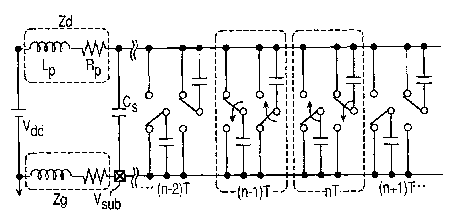
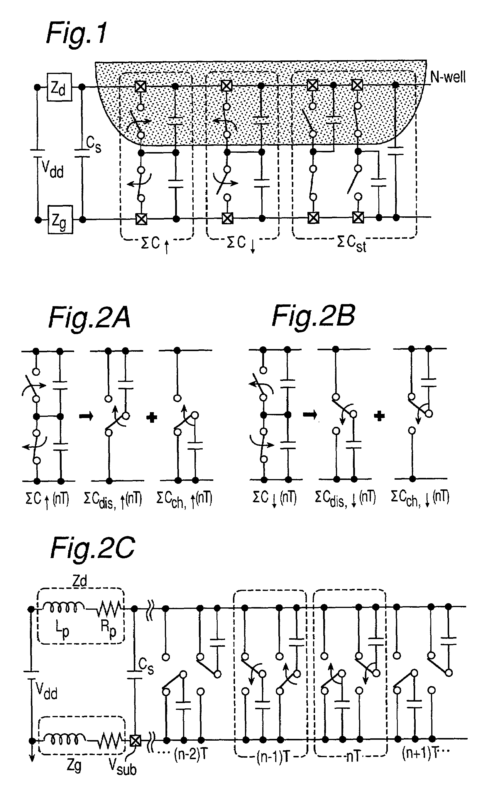
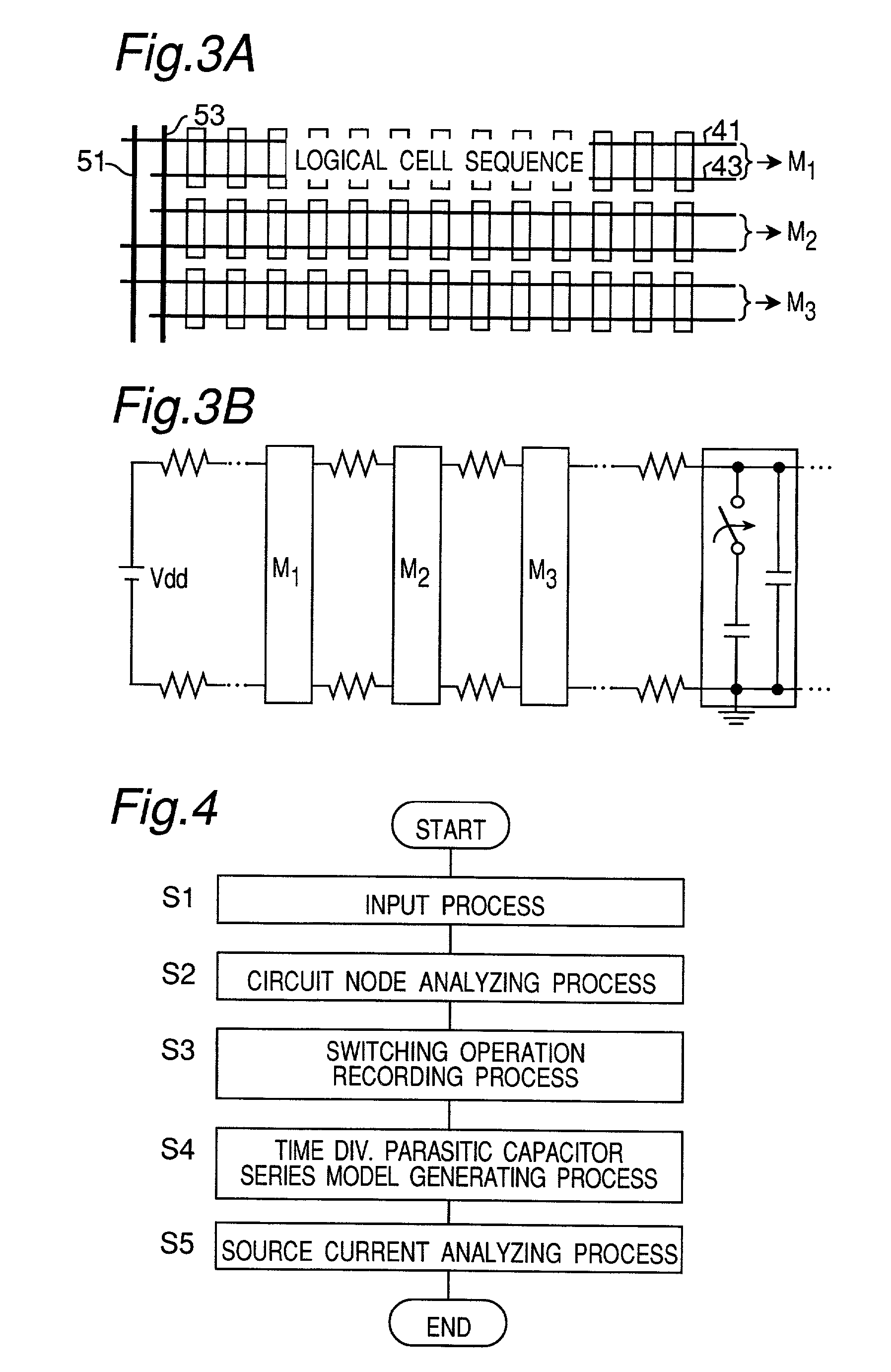
[0037]A method and an apparatus for analyzing the waveform of a source current will be described in the form of embodiments of the present invention will be described referring to the accompanying drawings.

[0038]The description starts with the concept of a source current analysis model using the method of analyzing the waveform of a source current according to the present invention.

[0039]The method of analyzing the waveform of a source current according to the present invention is based on the fact that the source current in a large-scale digital circuit depends significantly on a process of charging the load capacitance at the switching operation of each logic gate provided in the digital circuit. The method includes translating the large-scale digital circuit into a series of parasitic capacitors connected in time series between the power source and the ground according to a distribution of the switching operations of internal logic gates, and determining the waveform of a source ...


PUM


Abstract

The invention provides a method of analyzing a source current at a higher speed and an enhanced accuracy in a semiconductor integrated circuit including a digital circuit. The method to analyze a waveform of the source current, with consideration of re-distribution of charges throughout the digital circuit in the semiconductor integrated circuit, expressing the digital circuit with series of parasitic capacitors ΣCch, ↑ (nT) and ΣCch, ↓ (nT) to be charged and connected between the source and the ground lines. The capacitor series are calculated in time series based on the distribution of switching operations of the logic gates included in the digital circuit. An analysis model for determining the waveform of the source current in the digital circuit is obtained by connecting the parasitic capacitor series with a couple of respective parasitic impedances Zd and Zg of the source line and the ground line.

Description

BACKGROUND OF THE INVENTION[0001]1. Field of the Invention[0002]The present invention relates to a technology for designing a large-scale semiconductor integrated circuit, or particularly to a method of analyzing a source current across a logic circuit in a large-scale semiconductor integrated circuit and a technology for circuit designing with the method.[0003]2. Description of the Related Art[0004]As electronic devices in a large-scale integrated circuit (referred to as “LSI”, hereinafter) have been reduced in the size, digital circuits patterned in the LSI are scaled out and improved in an operation speed. However, such LSIs and their application systems generally suffer from degradation in the performance due to the generation of noises which results from a change in the source current flowing across the LSI circuits during the operation.[0005]FIG. 10 illustrates a mixed analog / digital integrated circuit (referred to as AD mixed LSI hereinafter). As shown, a single semiconductor...

Claims


Application Information

Patent Timeline
Patent Type & Authority Patents(United States)
IPC IPC(8): G06F17/00G01R29/26G01R13/00G01R31/30G01R31/316G06F17/50H01L21/82
CPCG06F17/5036G01R31/3004G06F30/367G01R13/00
Inventor NAGATA, MAKOTOIWATA, ATSUSHI
Owner A R TEC CORP
Why Eureka
Try Eureka