
Fluorinated hard mask for micropatterning of polymers

a technology of polymer film and hard mask, which is applied in the direction of photosensitive material processing, photomechanical equipment, instruments, etc., can solve the problems of inability to meet stringent specifications, inability to use traditional lithographic resists, and materials that are mostly not compatible with the fabrication process of integrated circuits, etc., to achieve the effect of increasing the chemical resistance of the polymer

Inactive Publication Date: 2006-05-09
INTERUNIVERSITAIR MICRO ELECTRONICS CENT (IMEC VZW)
View PDF9 Cites 7 Cited by
  • Summary
  • Abstract
  • Description
  • Claims
  • Application Information

AI Technical Summary

Benefits of technology

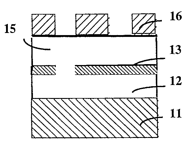
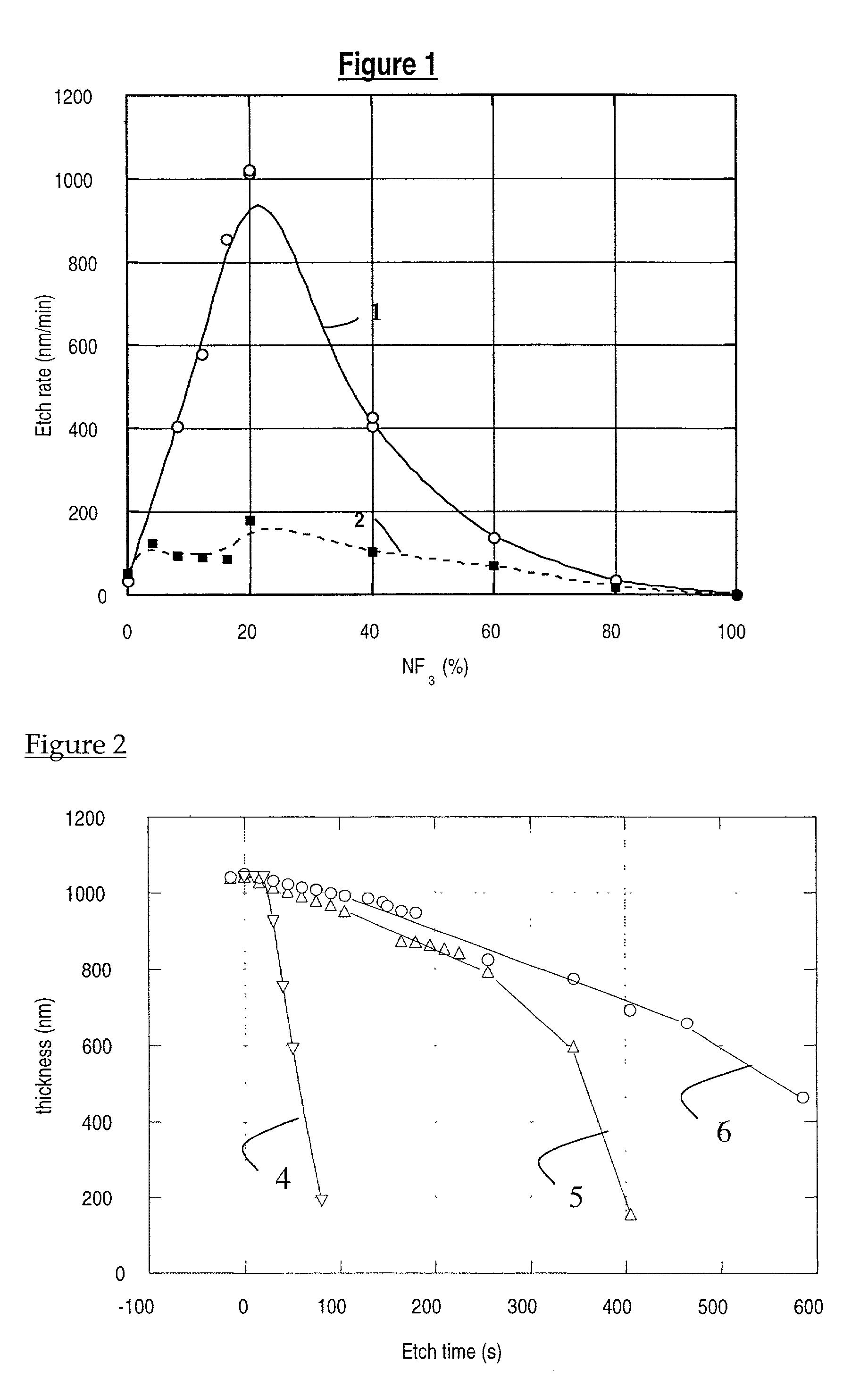
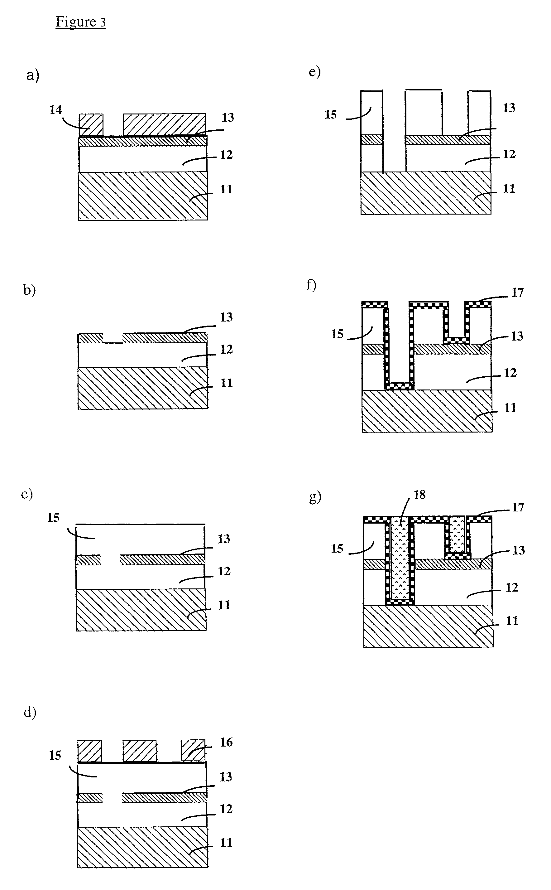
[0007]An aim of the present invention is to form a hard mask layer in an organic polymer layer by modifying at least locally the chemical composition of a part of an exposed organic low-K polymer. The polymer comprises phenyl groups. This modification starts from an exposed surface of the polymer and extends into the polymer thereby increasing the chemical resistance of the polymer. As a result, this modified part can be used as a hard mask for plasma etching. This modification is performed by exposing the low-K polymer to an ambient comprising fluorine, substantially without changing the film thickness, i.e., substantially without etching the low-K polymer. By doing so, the use of an extra hard mask layer, particularly an inorganic hard mask layer, can be avoided or at least removed subsequently. Furthermore, the mean K value even decreases due to the fluorination.
[0011]In another embodiment of the invention a method is disclosed, wherein the organic polymer comprises at least one phenyl group. Particularly, the organic polymer can be selected from a group comprising benzocyclobutarenes, poly arylene ether, aromatic hydrocarbon, and polyimides. Phenyl groups comprise carbon-hydrogen bonds, which can easily be attacked by reactive species, such as atomic fluorine generated in a plasma or other ambient comprising active fluorine. The active fluorine can abstract hydrogen from carbon in the phenyl groups. As a result, at least a part of the organic polymer layer is fluorinated leading to a lower permittivity value compared to a pristine one, and a higher chemical resistance especially in regard to an oxygen or an oxygen-fluorine based RIE (reactive ion etch) plasma.

Problems solved by technology

Conventionally, metal interconnects, mostly aluminum layers, with silicon dioxide as a dielectric are used, but this conventional solution will not be able to meet the stringent specifications resulting from the above mentioned trends.
The inorganic low-K materials have mostly interesting K values below 2 or even below 1.5 like, e.g., xerogels, but these materials are mostly not compatible with the fabrication process of integrated circuits.
Traditional lithographic resists are not suited to be used as hard mask layers for patterning organic low-K spin-on materials because these resists are also based on organic polymers resulting in an insufficient etch selectivity with regard to the organic low-K spin-on material.
These conventional inorganic hard mask layers have a rather high K value, i.e., typically in the range of 3.9 and above, which makes them less suitable for interconnect or isolation structures wherein the hard mask layers cannot be removed.

Method used


Image

  • Fluorinated hard mask for micropatterning of polymers
  • Fluorinated hard mask for micropatterning of polymers
  • Fluorinated hard mask for micropatterning of polymers

Examples


Embodiment Construction

[0017]In relation to the appended drawings, the present invention is described in detail. It is apparent, however, that a person skilled in the art can imagine several other equivalent embodiments or other ways of executing the present invention, the spirit and scope of the present invention being limited only by the terms of the appended claims.

[0018]In one aspect of the invention, a method is disclosed to form a hard mask layer in an organic polymer film by modifying at least partly the chemical composition of a first region of an organic polymer film comprising at least one phenyl group. Perferably, the first region is uncovered. If desirable, the first region can also be covered with suitable materials which do not adversely affect the fluorination of the polymer film. This modification is performed by exposing a surface of the organic polymer film to an ambient comprising fluorine substantially without changing the thickness of the first region of the organic polymer film. Phen...


PUM


Abstract

The present invention discloses the formation of a hard mask layer in an organic polymer layer by modifying at least locally the chemical composition of a part of said exposed organic low-k polymer. This modification starts from an exposed surface of the polymer and extends into the polymer thereby increasing the chemical resistance of the modified part of the polymer. As a result, this modified part can be used as a hard mask or an etch stop layer for plasma etching.

Description

RELATED APPLICATIONS[0001]This application is a division of application Ser. No. 09 / 085,691, filed May 27, 1998, now U.S. Pat. No. 6,245,489, which claims the benefit of priority under 35 U.S.C. §119(e) from Provisional Application No. 60 / 063,487, filed Oct. 22, 1997.FIELD OF THE INVENTION[0002]The present invention is directed to the patterning of organic polymer films comprising phenyl groups. These polymer films are used, e.g., as inter- or intra-dielectric layers in semiconductor device fabrication for isolation purposes in multi-metal layer structures.BACKGROUND OF THE INVENTION[0003]The increasing complexity of integrated circuits, the growing number of metal levels and the focus on increasing speed of these circuits have created demands for low permittivity materials, particularly for use as inter-metal layers, i.e., used to isolate two metal levels from one another, or intra-metal layers, i.e., used to isolate metal patterns possibly formed within the same metal level one fr...

Claims


Application Information

Patent Timeline
IPC IPC(8): H01L23/48H01L21/28G03F7/09G03F7/36G03F7/38G03F7/40H01L21/302H01L21/3065H01L21/311H01L21/768
CPCG03F7/094G03F7/36G03F7/38G03F7/40H01L21/31138H01L21/76829H01L21/7681H01L21/76822H01L21/76826H01L21/31144H01L21/76802H01L21/76801H01L21/76835
Inventor BAKLANOV, MIKHAIL RODIONOVICHVANHAELEMEERSCH, SERGEMAEX, KARENWAETERLOOS, JOOSTDECLERCK, GILBERT
Owner INTERUNIVERSITAIR MICRO ELECTRONICS CENT (IMEC VZW)
Learn More