High speed serial I/O technology using an optical link

a high-speed serial i/o technology and optical link technology, applied in the field of serial communication, can solve the problems of data link degradation at higher bandwidths, excessive noise and signal attenuation, and limited bandwidth capability of conventional data communication technologies, and achieve accurate, high-bandwidth connection, and minimize throughput degradation

Inactive Publication Date: 2006-05-16
XILINX INC
View PDF5 Cites 6 Cited by
  • Summary
  • Abstract
  • Description
  • Claims
  • Application Information

AI Technical Summary

Benefits of technology

[0010]The invention provides a high-speed optical transceiver for an IC by integrating optical transceiver components with the IC at the die level, thereby minimizing throughput degradation and simplifying the manufacturing process. According to an embodiment of the invention, a SERDES is attached to an IC using a covalent bonding technique. The covalent bond provides an accurate, high-bandwidth connection between the SERDES and IC. Furthermore, the strong covalent bond allows subsequent planarization and processing operations to be performed on the SERDES (and IC) without fear of damaging any data interconnections.

Problems solved by technology

However, conventional data communications technologies have a limited bandwidth capability. FIG. 1a shows a conventional printed circuit board (PCB) 100a, which comprises an integrated circuit (IC) 120 mounted on a board 110 (typically made from FR4).
Unfortunately, the data links degradation at higher bandwidths.
Typically, a copper trace on an FR4 board can sustain at most a 2 GHz signal—anything greater results in excessive noise and signal attenuation.
Increasing the number of traces to create a wider data path can provide some overall bandwidth improvement, but board area restrictions, EMI effects, and data synchronizing issues can reduce the effectiveness of this type of parallel bus structure.
Although optimized for high-speed data transmission, typical flex interconnects (such as those manufactured by MicroConnex Corp. and Flex Interconnect Technologies) still cannot sustain a data rate of much greater than 10 Gb / s.
Unfortunately, manufacturing electronics package 100b can be extremely expensive because each die (IC120, SERDES 130, and VCSEL / detector array 140) must be produced separately and then assembled into a single PCB.
This type of “package-level” integration is generally much more costly than a “die-level” integration due to the manual assembly operations required.

Method used


Image

  • High speed serial I/O technology using an optical link
  • High speed serial I/O technology using an optical link
  • High speed serial I/O technology using an optical link

Examples


Embodiment Construction

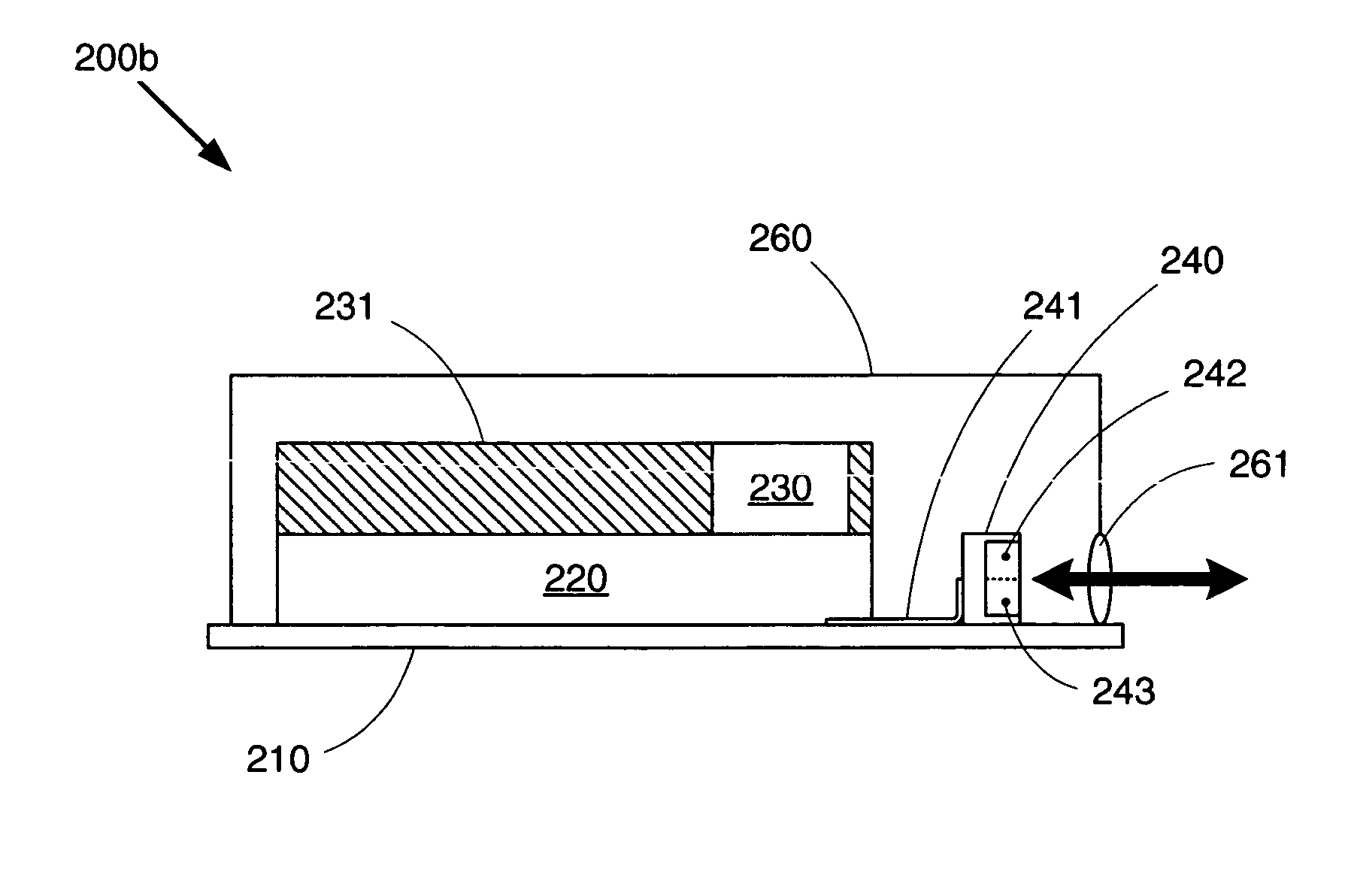
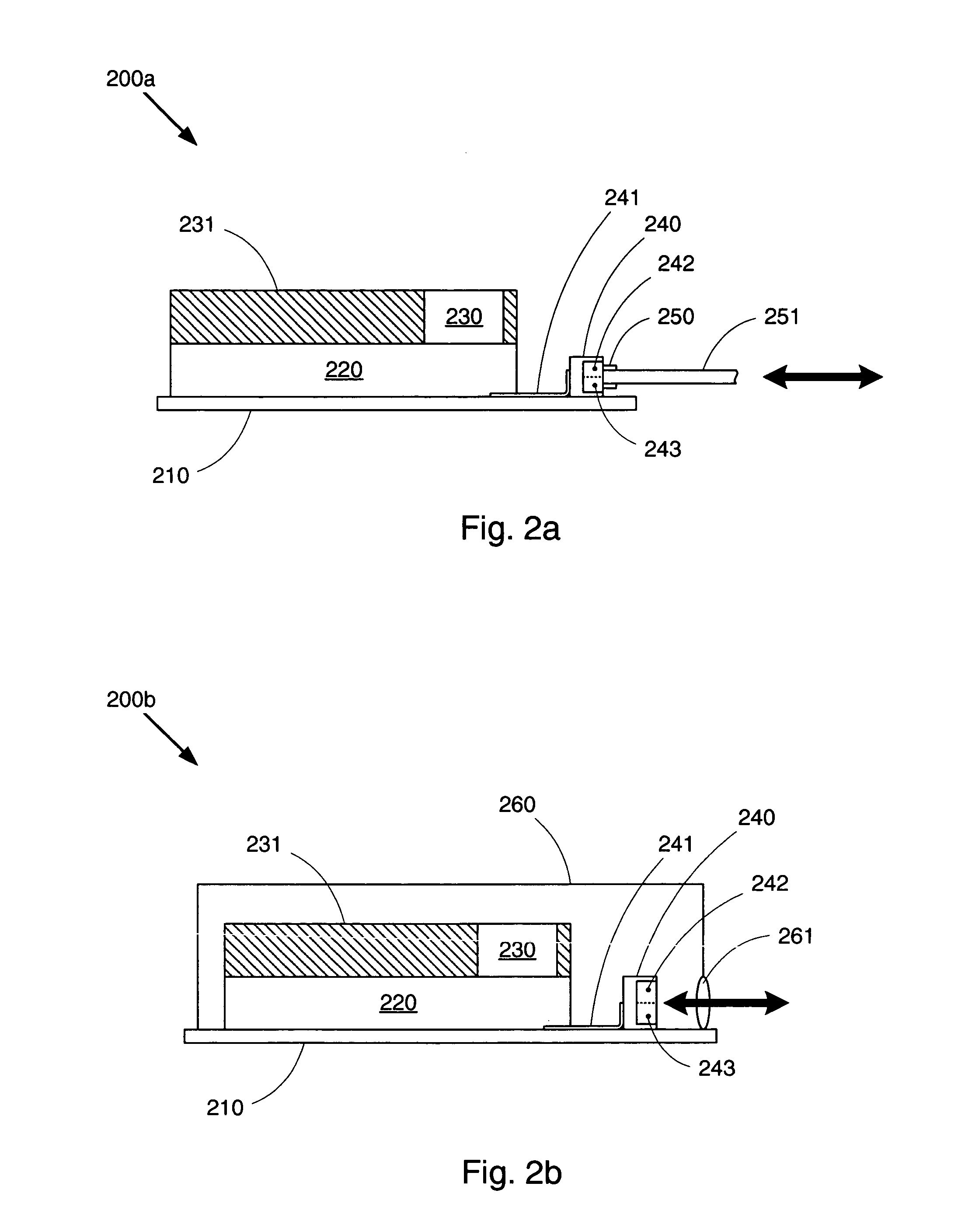
[0019]FIG. 2a shows an IC assembly 200a that incorporates an optical transceiver in accordance with an embodiment of the invention. IC assembly 200a comprises an IC 220 mounted on a support structure 210. IC 220 can comprise any type of IC, such as a field programmable gate array (FPGA), a microprocessor, or a memory module. Support structure 210 can comprise any structure onto which IC 220 can be mounted, including a PCB or a standard chip package. The optical communications capability of IC assembly 200a is provided by a SERDES 230 formed on IC 220 and an opto-electronic converter 240 connected to IC 220 via a flex interconnect 241. Opto-electronic converter 240 converts electrical signals to and from optical signals and therefore includes a transmitter 242 and a receiver 243. Transmitter 242 can comprise any device for providing the electrical-to-optical signal conversion, including a light-emitting diode (LED), a VCSEL, or even a light modulating device. Similarly, receiver 243 ...


PUM


Abstract

A high-speed optical transceiver for an integrated circuit (IC) includes a serializer-deserializer (SERDES) and a vertical cavity surface emitting laser (VCSEL) combined with a detector array. By covalently bonding the SERDES die to the IC, the two components can be processed simultaneously to produce a tightly aligned, high-speed data interface. The SERDES can be coupled to the VCSEL/detector array using a flex interconnect, or the VCSEL/detector array can also be covalently bonded to the IC or SERDES to maximize data bandwidth. The SERDES and VCSEL/detector array can also be produced in a single die using a process technology appropriate for both to maximize manufacturing efficiency.

Description

BACKGOUND OF THE INVENTION[0001]1. Field of the Invention[0002]The invention relates to serial communications between electronic components, and more particularly to a high-speed optical communications link.[0003]2. Discussion of Related Art[0004]As the bandwidth requirements of modern microprocessors and other electronic devices continue to increase, the need for a high-speed, low-noise communications technique becomes more and more important. In the near future, data transfer rates in excess of 40 Gb / s will be required to keep up with the faster CPU clock speeds. However, conventional data communications technologies have a limited bandwidth capability. FIG. 1a shows a conventional printed circuit board (PCB) 100a, which comprises an integrated circuit (IC) 120 mounted on a board 110 (typically made from FR4). A copper trace 111 printed on board 110 routes signals to and from IC 120. PCB 100a is installed in a socket 191 of a backplane 190. Copper trace 111 interfaces with socket ...

Claims


Application Information

Patent Timeline
Patent Type & Authority Patents(United States)
IPC IPC(8): G02B6/36H01L21/00H04B17/00G02B6/43
CPCG02B6/43
Inventor GRUNG, BERNARD L.WALTERS, WAYNE L.BAIER, STEVEN M.
Owner XILINX INC
Why Eureka
Try Eureka