Liquid crystal display apparatus

Inactive Publication Date: 2006-05-16
HITACHI LTD
View PDF15 Cites 17 Cited by
  • Summary
  • Abstract
  • Description
  • Claims
  • Application Information

AI Technical Summary

Benefits of technology

[0019]The patterned insulating film of the present invention is composed in a manner such that the patterned insulating film is formed between the gate insulating film and the organic semiconductor layer, and regions of the insulating film above or beneath the gate electrode are removed. The area of the region of the insulating film to be removed desirably has the same size as the size of the gate electrode. The patterned insulating film has a function as a mask pattern when forming the semiconductor film. That is, the semiconductor layer can be formed so as to contact the gate insulating film only in the regions, which operate as channel regions, by accumulating the semiconductor film onto the patterned insulating film after forming the patterned insulating film. The se

Problems solved by technology

With respect to a conventional organic TFT, the organic semiconductor film can not be manufactured finely, and the area of the organic semiconductor film is larger than the gate electrodes.
If the on/off ratio is decreased, for ins

Method used


Image

  • Liquid crystal display apparatus
  • Liquid crystal display apparatus
  • Liquid crystal display apparatus

Examples


embodiment 1

(Embodiment 1)

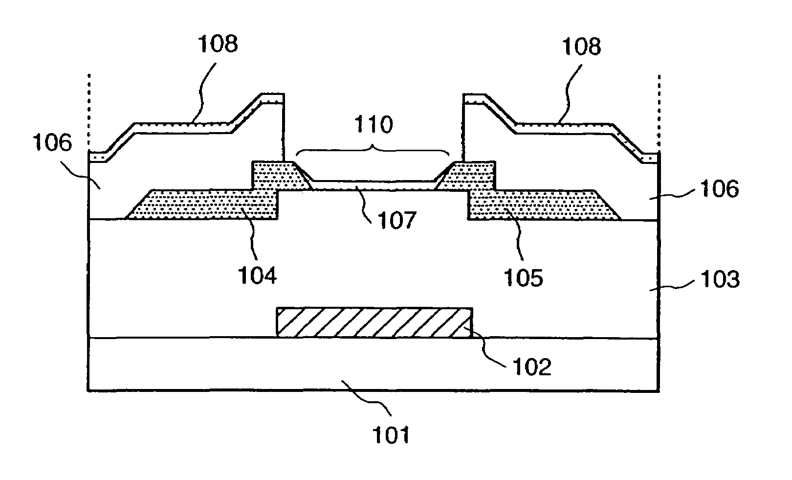
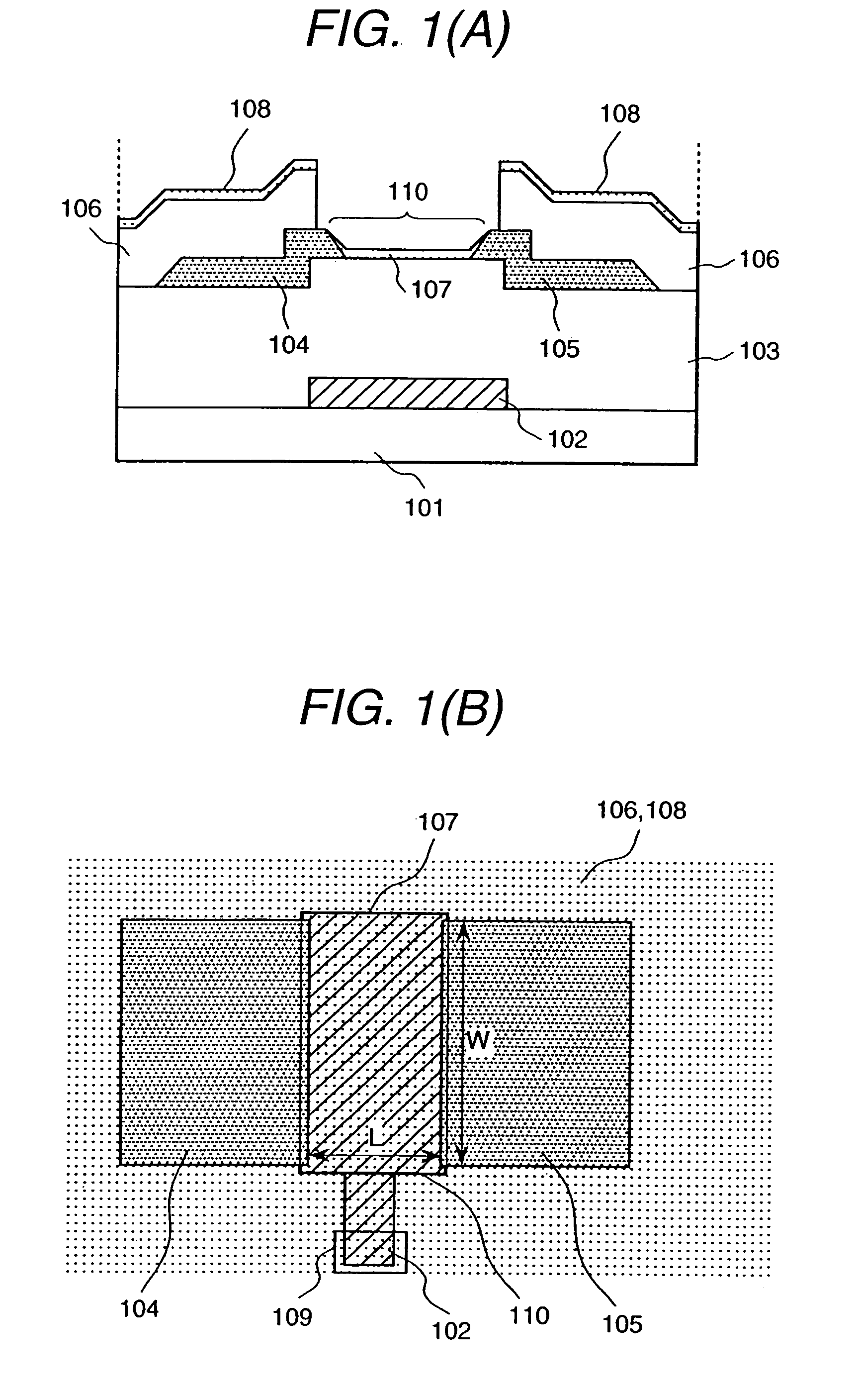
[0035]Hereinafter, details of the organic TFT of the present invention is explained referring to FIG. 1 and FIG. 2.

[0036]FIG. 1(A) is a schematic cross sectional view of the organic TFT element of embodiment 1 of the present invention. FIG. 1(B) is a schematic plan view of the organic TFT element of embodiment 1 of the present invention. The organic TFT element has a glass substrate 101, a gate electrode 102, a gate insulating film 103, a source electrode 104, a drain electrode 105, a patterned insulating film 106, a conjugated sexithiophene oligomer (a-6T) organic semiconductor film 107 in the channel region, a-6T (a-6T) organic semiconductor film 108 in the non-channel region, an opening 109 for taking out the gate electrode, and a region 110 where the patterned insulating film is removed. That is, the patterned insulating film 106 is composed so as to be formed between the gate insulating film 103 and the organic semiconductor layer (organic semiconductor film 107),...

embodiment 2

(Embodiment 2)

[0047]Next, an embodiment of the TFT element of the present invention, wherein a photosensitive organic insulating film is used as the patterned insulating film, will be explained with reference to FIG. 3(A), FIG. 3(B), FIG. 4(A) and FIG. 4 (B).

[0048]FIG. 3(A) is a schematic cross sectional view of the structure of the organic TFT element representing an embodiment 2. FIG. 3(B) is a partial plan view of the structure of the organic TFT element in the embodiment 2. The organic TFT element has a glass substrate 301, a gate electrode 302, a gate insulating film 303, a source electrode 304, a drain electrode 305, a patterned insulating film 306 made of a photosensitive organic insulating film, a a-6T organic semiconductor film 307 in a channel region, the a-6T organic semiconductor film 308 in a non-channel region, an opening 309 for taking out the gate electrode, and a region 310 where the photosensitive organic insulating film has been removed. That is, the patterned ins...

embodiment 3

(Embodiment 3)

[0055]Next, an embodiment, wherein the organic TFT element relating to the present invention is used in an active matrix liquid crystal display apparatus, will be explained with reference to FIG. 5 to FIG. 7.

[0056]FIG. 5 illustrates an active matrix liquid crystal display apparatus relating to the present invention. FIG. 6 is a schematic cross sectional view of the active matrix liquid crystal display apparatus taken along the line A–A′ in FIG. 5. The apparatus has a glass substrate 501, a gate electrode 502, a gate insulating film 503, a source electrode 504, a drain electrode 505, a patterned insulating film 506, an a-6T organic semiconductor film 507 in the channel region, an a-6T organic semiconductor film 508 in the non-channel region, signal lines 509 and 509, a scanning line 510, a pixel electrode 511, a SiOX protection film 512, orientation films 513 and 513, a counter electrode 515, a liquid crystal composition 516, a spacer bead 517, polarizers 518 and 518′, ...


PUM

PropertyMeasurementUnit
Sizeaaaaaaaaaa
Plasticityaaaaaaaaaa
Photosensitivityaaaaaaaaaa

Abstract

The present invention provides a thin film transistor, wherein the semiconductor channel region is patterned. Gate electrodes 102, gate insulating film 103, source electrodes 104, and drain electrodes 105 are formed on a glass substrate 101. A patterned insulating film is formed thereon, and a part of the film in the region 110 on the gate electrode is removed. An organic semiconductor film is formed thereon by vapor deposition. The organic semiconductor film 107 in the region 110, where the patterned insulating film is removed, becomes a channel region, and is separated from the organic semiconductor film 108 on the patterned insulating film 106. Therefore, the organic semiconductor channel region is patterned to have the same size as the gate electrode. In accordance with the present invention, a thin film transistor, wherein the semiconductor region is patterned precisely, becomes available.

Description

[0001]This application is a Continuation application of application Ser. No. 09 / 949,091, filed Sep. 10, 2001, U.S. Pat. No. 6,593,977 which is a Continuation application of application Ser. No. 09 / 526,557, filed Mar. 16, 2000, U.S. Pat. No. 6,300,988 the contents of which are incorporated herein by reference in their entirety.BACKGROUND OF THE INVENTION[0002]The present invention relates to a liquid crystal display apparatus, particularly, to an active matrix liquid crystal display apparatus and IC (Integrated Circuit) cards.[0003]Currently, an active matrix liquid crystal display apparatus using active elements, represented by TFT (Thin Film Transistor) devices, have been widely used as monitors for personal computers and work stations, in view of their high image quality, which is comparable to a CRT (Cathode Ray Tube), their low power consumption, which is less than a CRT, and saving space. However, an active matrix liquid crystal display apparatus is expensive in comparison with...

Claims


Application Information

Patent Timeline
IPC IPC(8): H01L29/04H01L35/24H01L51/05G02F1/136G02F1/1368H01L21/311H01L21/336H01L27/28H01L29/49H01L29/786H01L51/00
CPCG02F1/1368H01L29/4908H01L51/0545H01L51/0002H01L51/0014H01L51/0525H01L29/78696H01L21/31116H01L27/283H01L51/0036H10K19/10H10K71/10H10K71/20H10K85/113H10K10/472H10K10/466G02F1/136
Inventor ISHIHARA, SHINGOWAKAGI, MASATOSHIANDO, MASAHIKO
Owner HITACHI LTD
Why Eureka
Try Eureka