Method for selecting and placing bypass capacitors on multi-layer printed circuit boards

a multi-layer printed circuit board and bypass capacitor technology, applied in cross-talk/noise/interference reduction, program control, instruments, etc., can solve the problems of electronic components generating an increasing level of noise, the purpose of controlling high-frequency transient noise is limited, and the electronic circuit becomes more complex. , to achieve the effect of signal transmission line reflection and noise control

Active Publication Date: 2006-05-16
EXTREME NETWORKS INC
View PDF9 Cites 30 Cited by
  • Summary
  • Abstract
  • Description
  • Claims
  • Application Information

AI Technical Summary

Benefits of technology

[0026]By use of the bypass capacitors on multi-layer printed circuit boards, the total area of the current loop formed by the signal trace and its return current can be minimized. Signal integ

Problems solved by technology

As electronic circuits become more complex and use a larger number of components, printed circuit boards must typically accommodate more electronic components in the same surface area.
As larger number of electronic components are used and densely located on printed circuit boards, these electronic components generate an increasing level of noise associated with power distribution among the electronic components.
Embedded capacitance is more effective at higher frequencies than local decoupling or bulk decoupling, but its purpose is limited to controlling high frequency transient noise on the power/ground distribution generated by active devices.
Therefore, the conventional decoupling capacitor placement does not control the noise generated by the specific signal path (also referred to as “signal traces”) of interconnecting routes between active devices.
On modern printed circuit boards with multiple supply voltages and ground pla

Method used


Image

  • Method for selecting and placing bypass capacitors on multi-layer printed circuit boards
  • Method for selecting and placing bypass capacitors on multi-layer printed circuit boards
  • Method for selecting and placing bypass capacitors on multi-layer printed circuit boards

Examples


first embodiment

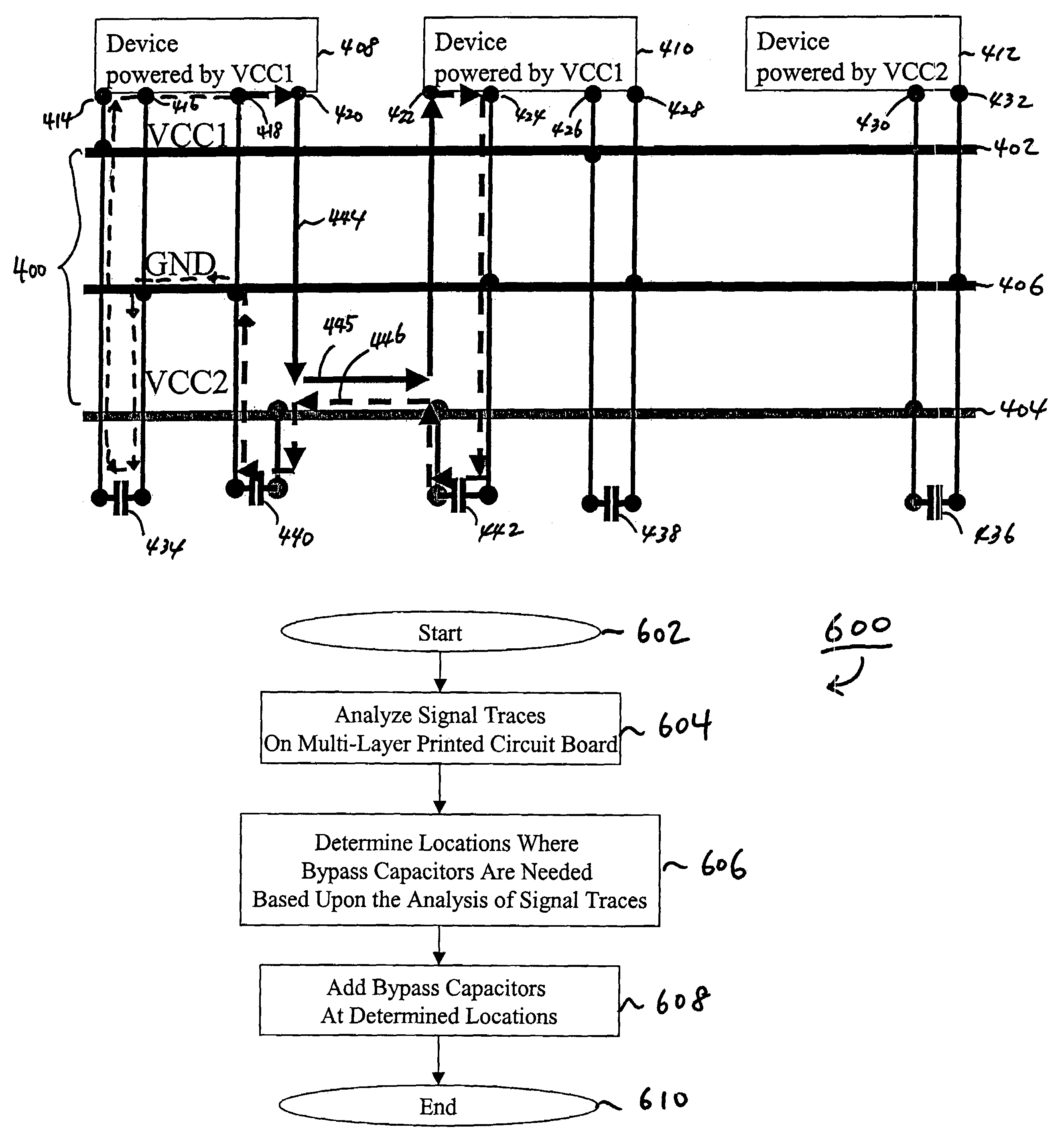
[0036]FIG. 4 is a diagram illustrating a multi-layer printed circuit board 400 in accordance with the present invention. The printed circuit board 400 shown in FIG. 4 is different from the conventional printed circuit board 200 shown in FIG. 2 in that additional bypass capacitors 440 and 442 were added. The printed circuit board 400 includes four layers, a Vcc1 supply voltage plane 402, a Vcc2 supply voltage plane 404, a GND plane 406 with conventional local decoupling capacitors 434, 436, 438, and a routing layer in which the signal current 445 flows. Two active devices, device 408 (driver part), device 410 (receiver part), and another active device 412 (unrelated to devices 408 and 410) are shown placed on the printed circuit board 400. The devices 408, 410, 412 may be any type of device such as an active integrated circuit (IC) chip or a discrete component. Device 408 has at least four pins 414, 416, 418, 420, device 410 has at least four pins 422, 424, 426, 428, and device 412 h...

second embodiment

[0042]FIG. 5 is a diagram illustrating a multi-layer printed circuit board 500 according to the present invention. The printed circuit board 500 of the present invention shown in FIG. 5 is different from the conventional printed circuit board 300 shown in FIG. 3 in that additional bypass capacitors 534, 536, 538, 540 according to the present invention were added. The printed circuit board 500 includes six layers, a Vcc1 supply voltage plane 502, a Vcc2 supply voltage plane 506, and a first GND plane 504, a second GND plane 508 with conventional local decoupling capacitors 530, 532, and two routing layers in which the signal currents 541, 542, 543 flows. Two active devices, device 510 (driver part) and device 512 (receiver part) are placed on the printed circuit board 500. The devices 510, 512 may be any type of device such as an integrated circuit (IC) chip or a discrete component. Device 510 has at least four pins 514, 516, 518, 520, and device 512 has at least four pins 522, 524, ...


PUM


Abstract

A method places bypass capacitors for controlling the signal integrity of a signal routed between devices on a multi-layer printed circuit board by analysis of the routing of the signal and the signal characteristics. In general, when an interconnecting signal between devices is routed adjacent to an impedance control plane that does not serve as the circuit supply voltage plane or the reference voltage plane for all devices interconnected by the signal trace, the method selects locations for addition of bypass capacitors based upon the routing of the interconnecting signal trace to improve signal integrity.

Description

TECHNICAL FIELD[0001]The present invention relates generally to controlling electronic noise in multi-layer printed circuit boards, and more specifically, to a method for selecting and placing bypass capacitors on multi-layer printed circuit boards in order to control noise and improve signal integrity.BACKGROUND OF THE INVENTION[0002]Multi-layer printed circuit boards are widely used in modern electronics technology to interconnect various components in a compact and efficient manner. These components include active Integrated Circuits (ICs) or passive discrete components (resistors, capacitors, and the like). As electronic circuits become more complex and use a larger number of components, printed circuit boards must typically accommodate more electronic components in the same surface area. As a result, electronic components have become densely located and modern printed circuit boards use multiple layers to provide various supply and return voltages such as 5 V, 3.3 V, and Ground...

Claims


Application Information

Patent Timeline
IPC IPC(8): G06F17/50
CPCG06F17/5072H05K1/0231H05K2201/09309H05K3/0005H05K1/0298G06F30/392
Inventor VITEK, CLARK A.BHANDARI, NITIN
Owner EXTREME NETWORKS INC
Why Eureka
Try Eureka