Method for enhancing silicon dioxide to silicon nitride selectivity

Inactive Publication Date: 2006-05-23
ROUND ROCK RES LLC
View PDF122 Cites 50 Cited by
  • Summary
  • Abstract
  • Description
  • Claims
  • Application Information

AI Technical Summary

Benefits of technology

[0018]The present invention provides unexpected and very key improvements over the current etch processes. The present invention teaches away from current thought, by usin

Problems solved by technology

With geometries shrinking, it is becoming more difficult to align small contacts in between closely spaced wordlines or other conductive structures.
Higher density multilayer structures such as 64 and 256 Megabit DRAM require an additional amount of alignment tolerance which can not be addressed by current photolithographic means.
A problem of profile control occurs with respect to etching of a multilayer structure having a silicon dioxide layer disposed o

Method used


Image

  • Method for enhancing silicon dioxide to silicon nitride selectivity
  • Method for enhancing silicon dioxide to silicon nitride selectivity
  • Method for enhancing silicon dioxide to silicon nitride selectivity

Examples


Embodiment Construction

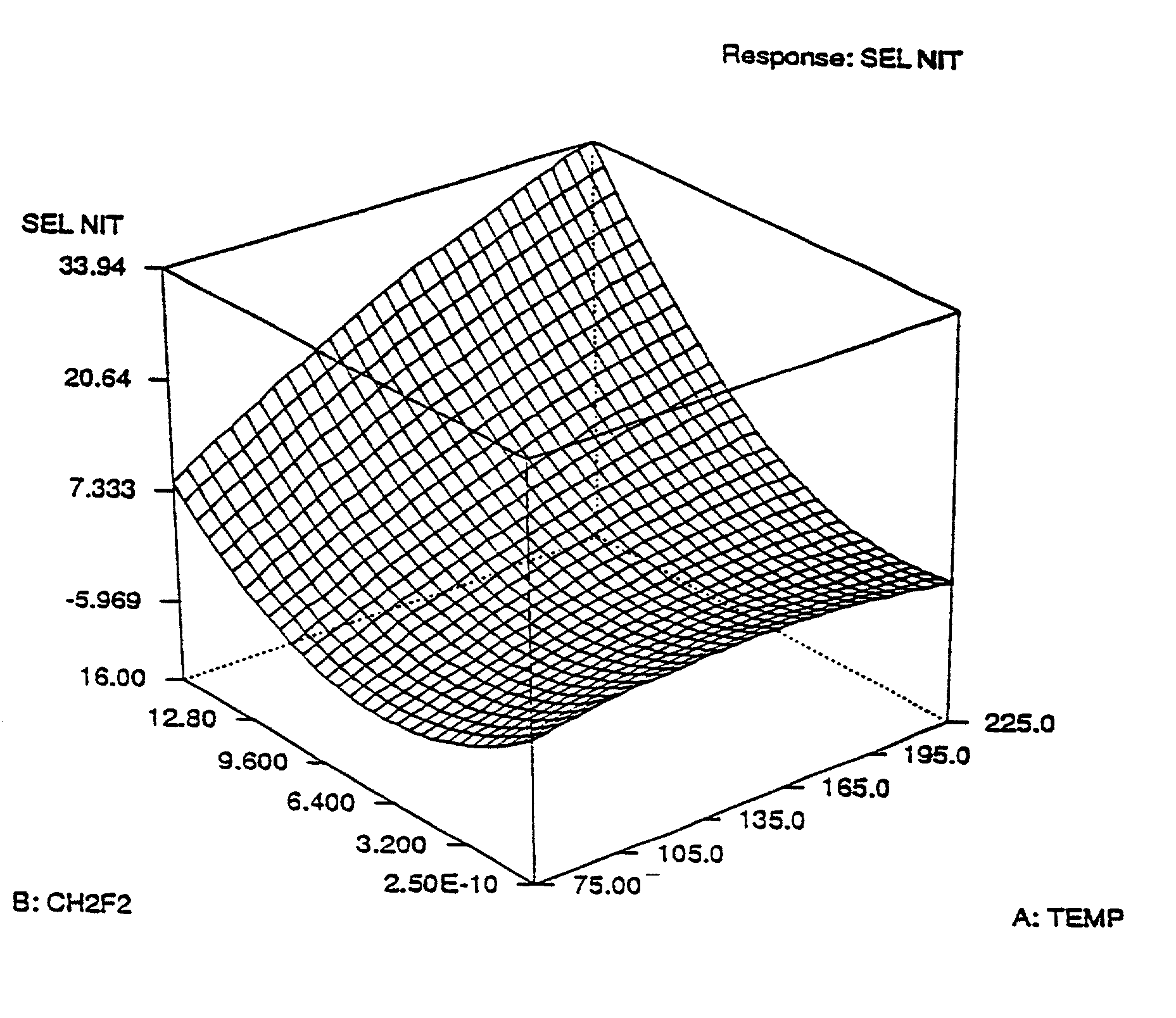
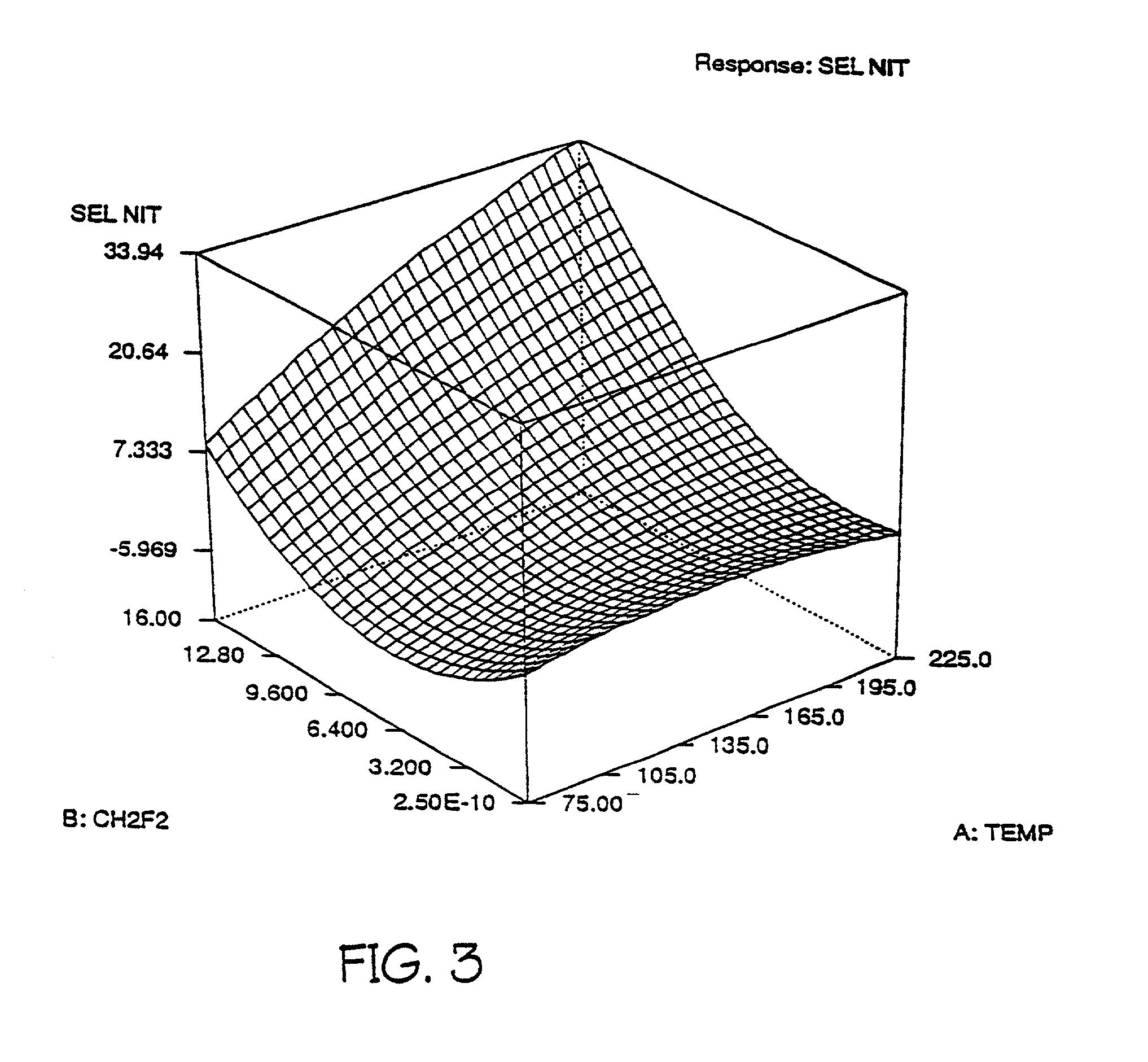
[0025]The inventive process herein is directed towards anisotropically etching a multilayer structure comprising a silicon dioxide outer layer on an underlying silicon nitride “stop” layer.

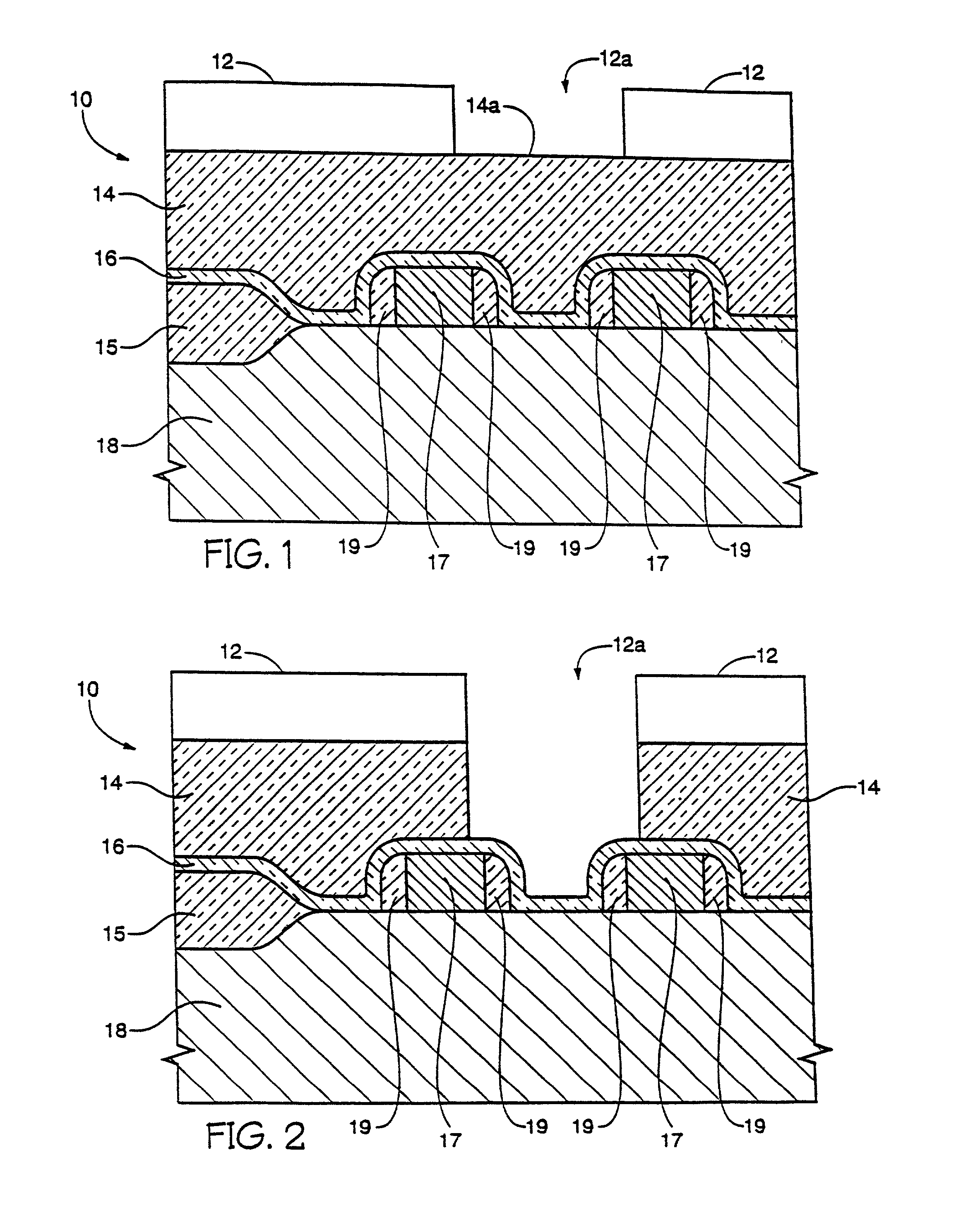
[0026]Referring to FIG. 1, a multilayer structure, which is formed by conventional techniques, is depicted. It will serve as a representative example. The multilayer structure of FIG. 1, generally designated as 10, is shown prior to etching.

[0027]The multilayer structure 10 comprises a plurality of structural layers which are sequentially disposed on an underlying silicon structure or wafer 18. Multilayer structure 10 comprises a plurality of structural layers including a layer 14 having a major outer surface 14a. Structural layer 14 is fabricated of SiO2.

[0028]Generally, an undoped oxide 15, referred to as a field oxide or gate oxide, is usually grown in a furnace. Doped oxide includes BPSG, PSG, etc. which are generally deposited on the silicon wafer with a dopant gas (es) during a deposition pr...


PUM

PropertyMeasurementUnit
Temperatureaaaaaaaaaa
Selectivityaaaaaaaaaa
Etch rateaaaaaaaaaa

Abstract

A process for controlling the plasma etch of a silicon dioxide layer at a high etch rate and high selectivity with respect to silicon nitride, particularly in a multilayer structure, by (1) maintaining various portions of the etch chamber at elevated temperatures, and/ox (2) using an etch chemistry having a fluorohydrocarbon gas containing at least as many hydrogen atoms as fluorine atoms, preferably CH2F2 or CH3F.

Description

CROSS-REFERENCE TO RELATED APPLICATIONS[0001]This is a continuation application of U.S. application Ser. No. 09 / 344,277, filed Jun. 30, 1999, which issued as U.S. Pat. No. 6,287,978 on Sep. 11, 2001; which was a continuation of U.S. applicant Ser. No. 08 / 905,891, filed Aug. 4, 1997, which issued as U.S. Pat. No. 6,015,760 on Jan. 18, 2000; which was a continuation of U.S. application Ser. No. 08 / 152,755, filed Nov. 15, 1993, which issued as U.S. Pat. No. 5,880,036 on Mar. 9, 1999; which was a continuation-in-part of U.S. application Ser. No. 07 / 898,505, filed Jun. 15, 1992, which issued as U.S. Pat. No. 5,286,344 on Feb. 15, 1994.FIELD OF THE INVENTION[0002]This invention relates to semiconductor manufacturing, and more particularly to a process for selectively etching a silicon dioxide layer disposed on a silicon nitride layer, useful when etching features have submicron geometries.BACKGROUND OF THE INVENTION[0003]With geometries shrinking, it is becoming more difficult to align sm...

Claims


Application Information

Patent Timeline
IPC IPC(8): H01L21/302H01L21/311H01L21/768
CPCH01L21/76802H01L21/31116
Inventor BECKER, DAVID S.BLALOCK, GUY T.ROE, FRED L.
Owner ROUND ROCK RES LLC
Why Eureka
Try Eureka