High mobility heterojunction complementary field effect transistors and methods thereof

a complementary field effect and heterojunction technology, applied in the field of high mobility heterojunction complementary field effect transistors and field effect devices, can solve the problems of increasing complexity of technology, increasing the difficulty of silicon mos scaling, and traditional techniques failing to reduce certain undesirable physical effects

Inactive Publication Date: 2006-06-06
GLOBALFOUNDRIES US INC
View PDF6 Cites 154 Cited by
  • Summary
  • Abstract
  • Description
  • Claims
  • Application Information

AI Technical Summary

Benefits of technology

[0007]The present invention describes heterojunction source / drain MOSFET devices in which the PMOS is a buried SiGe channel device, while the NMOS is a surface silicon channel device. According to one aspect of the invention, the heterojunction and metallurgical junction of the device substantially coincide to within a close tolerance. Another aspect of the invention relates to a method comprising forming heterojunction source / drain by epitaxial deposition. The new heterojunction source / drain MOSFET devices can be realized in silicon on insulator (SOI), or in bulk Si technologies. The SiGe epitaxial source / drain will be compressively-strained due to lattice constant mismatch between Si and SiGe. Also, since the hole current in the PMOS will be primarily confined to a buried compressively strained SiGe channel, due to the high hole mobility in such a materials, this PMOS device can have potentially similar current carrying capability as the NMOS device. The high quality PMOS leads to excellent CMOS circuit capabilities for building processors.

Problems solved by technology

As MOS (Metal Oxide Semiconductor Field-Effect-Device, a name with historic connotations meaning in general an insulated gate Field-Effect-Device) devices are being scaled down, the technology becomes more complex and new methods are needed to maintain the expected performance enhancement from one generation of devices to the next.
Silicon MOS scaling has become a major challenge in the semiconductor industry.
Traditional techniques start to fail in reducing certain undesirable physical effects as device dimensions shrink down to the nanometer regime.
However, the abrupt doping profiles are difficult to achieve due to temperature enhanced diffusion, and these highly doped channels or pocket implant regions not only increase junction capacitance and band-to-band tunneling, but also degrades carrier mobility in the channel.
Hitherto there was no method to give the desired coincidence of the heterojunction and the metallurgical junction, and no lateral device structure with such coincidence has been disclosed.

Method used


Image

  • High mobility heterojunction complementary field effect transistors and methods thereof
  • High mobility heterojunction complementary field effect transistors and methods thereof
  • High mobility heterojunction complementary field effect transistors and methods thereof

Examples


Embodiment Construction

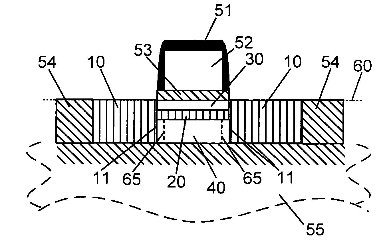
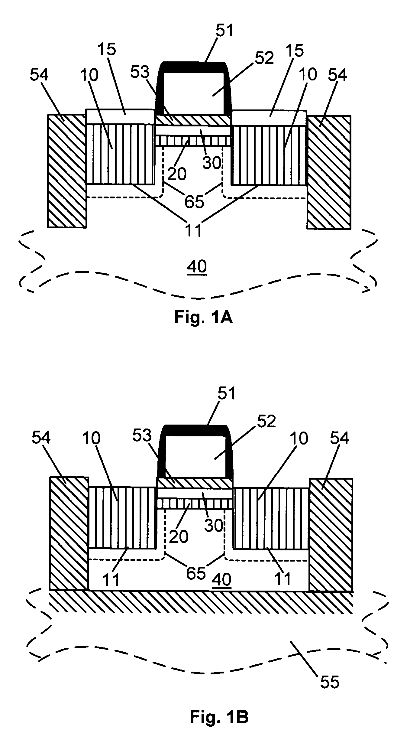
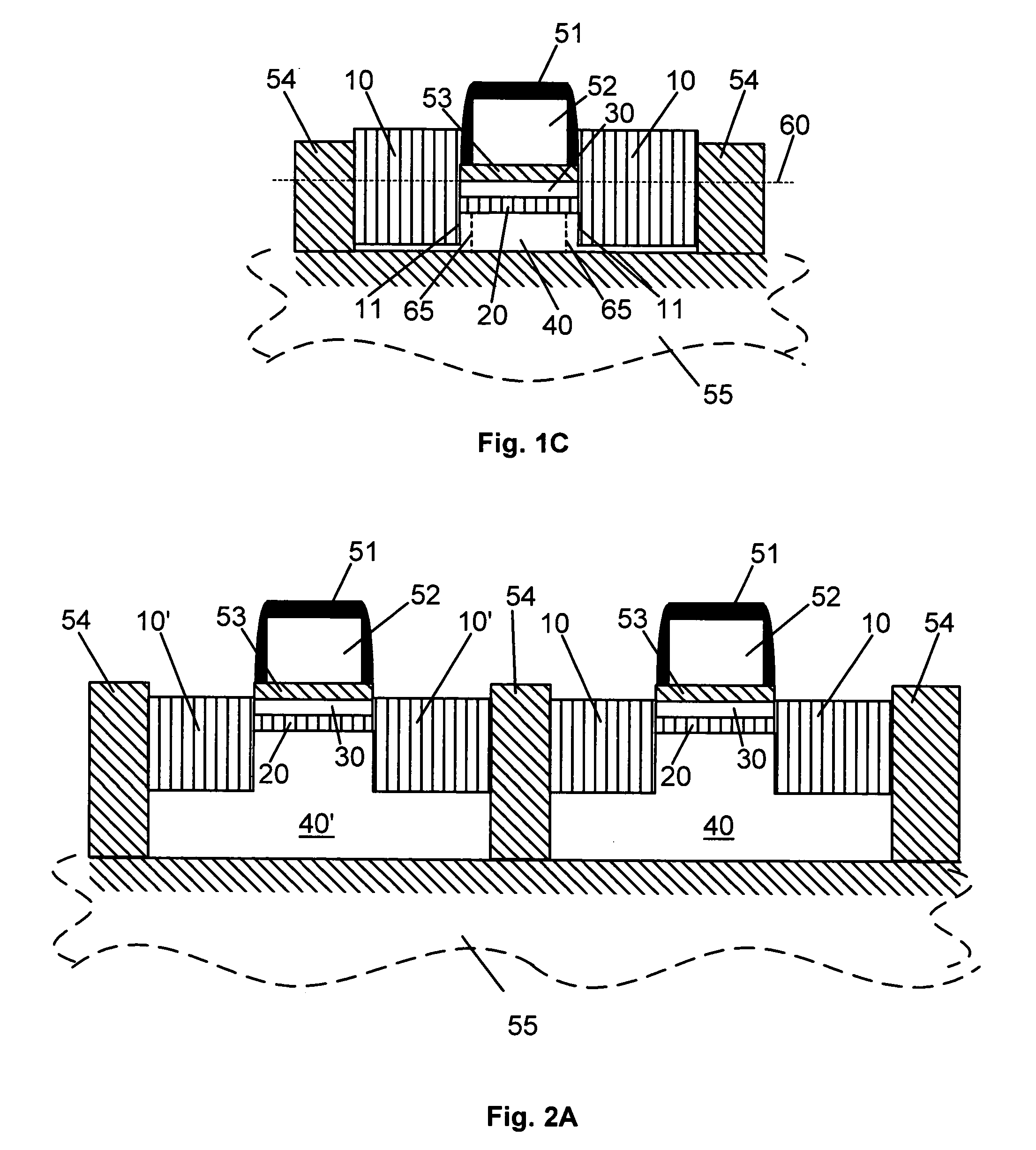
[0017]FIG. 1 schematically shows exemplary embodiments of a Si based heterojunction source / drain field device. Each embodiment contains the feature of the source 10 and drain 10 of the field effect device (FET) forming a heterojunction with the body 40 of the device. As every FET, the device has (at least one) gate 52. The conductive gate 52 in state of the art technologies is protected by a cover layer 51, which in Si based technologies is typically oxide and SiN. The gate 52 is electrically isolated from the rest of the device by the gate dielectric 53. The common property of FET-s is that the gate 52, by capacitive coupling across the gate insulator 53, controls the flow of the device current between the source 10 and drain 10. Insulator regions 54 serve for isolating the device. Typically the isolation is accomplished by shallow trenches 54, usually made of SiO2, as shown in the figures.

[0018]The material of the structure shown on FIG. 1 belongs in the broad category of Si based...


PUM


Abstract

In all representative embodiments presented, the Ge concentration in the source and drain 10 and the SiGe epitaxial channel layer 20 is in the 15% to 50% range, preferably between about 20% to 40%. The SiGe thicknesses in the source / drain 10 are staying below the critical thickness for the given Ge concentration. The critical thickness is defined such that above it the SiGe will relax and defects and dislocations will form. The thickness of the SiGe epitaxial layer 20 typically is between about 5nm and 15nm. The thickness of the epitaxial Si layer 30 is typically between about 5nm and 15nm. FIG. 1A shows an embodiment where the body is bulk Si. These type of devices are the most common devices in present day microelectronics. FIGS. 1B and 1C show representative embodiment of the heterojunction source / drain FET device when the Si body 40 is disposed on top of an insulating material 55. This type of technology is commonly referred to as silicon on insulator (SOI) technology. The insulator material 55 usually, and preferably, is SiO2. FIG. 1B shows an SOI embodiment where the body 40 has enough volume to contain mobile charges. Such SOI devices are called partially depleted devices. FIG. 1C shows an SOI embodiment where the volume of the body 40 is insufficient to contain mobile charges. Such SOI devices are called fully depleted devices. For devices shown in FIG. 1B and 1C there is, at least a thin, layer of body underneath the source and drain 10. This body material serves as the seed material onto which the epitaxial SiGe source and drain 10 are grown. In an alternate embodiment, shown in FIG. 1D. for extremely thin fully depleted SOI devices, one could grow the source and drain 10 laterally, from a lateral seeding, in which case the source and drain 10 would penetrate all the way down to the insulating layer 55.

Description

FIELD OF THE INVENTION[0001]The present invention relates to electronic devices and systems. In particular it relates to field effect devices, and a method of producing such structures, with a heterojunction source / drain which substantially coincides with the metallurgical junction between the source / drain and the device body.BACKGROUND OF THE INVENTION[0002]Today's integrated circuits include a vast number of devices. Smaller devices are key to enhance performance and to improve reliability. As MOS (Metal Oxide Semiconductor Field-Effect-Device, a name with historic connotations meaning in general an insulated gate Field-Effect-Device) devices are being scaled down, the technology becomes more complex and new methods are needed to maintain the expected performance enhancement from one generation of devices to the next.[0003]Silicon MOS scaling has become a major challenge in the semiconductor industry. Traditional techniques start to fail in reducing certain undesirable physical ef...

Claims


Application Information

Patent Timeline
Patent Type & Authority Patents(United States)
IPC IPC(8): H01L29/778H01L27/08H01L21/20H01L21/336H01L21/8238H01L27/092H01L29/10H01L29/78H01L29/786
CPCH01L21/823807H01L21/823814H01L29/66636H01L29/1054H01L29/7841H01L21/18
Inventor OUYANG, QIQING CHRISTINECHEN, XIANGDONG
Owner GLOBALFOUNDRIES US INC
Why Eureka
Try Eureka