A/D converter and A/D converting system

a converter and converter technology, applied in transmission systems, analogue/digital conversion, instruments, etc., can solve the problems of reducing the conversion accuracy of a/d, increasing the power consumption and an area of the circuit, and known a/d converters have disadvantages, so as to achieve the effect of increasing the conversion accuracy and increasing the conversion accuracy

Inactive Publication Date: 2006-06-13
PANASONIC CORP
View PDF7 Cites 16 Cited by
  • Summary
  • Abstract
  • Description
  • Claims
  • Application Information

AI Technical Summary

Benefits of technology

[0010]It is an object of the present invention to suppress, in a flash A / D converter, mismatch between an output dynamic range for differential amplifier circuits and an input dynamic range for voltage comparator circuits due to changes in fabrication processes for a semiconductor device with a simple configuration, thereby improving A / D conversion accuracy.
[0025]As has been described, according to the present invention, the regulator circuit regulates an output range including non-inversion or inversion output voltages of each differential amplifier circuit. Thus, even when variations in the output range of each differential circuit occur due to changes in fabrication processes for a semiconductor device, the output range of each differential amplifier circuit is in the input range of each voltage comparative circuit, so that A / D conversion accuracy is increased.
[0026]Specifically, in one embodiment of the present invention, when the regulator circuit regulates a common mode voltage of each differential amplifier circuit so that the common mode voltage becomes a reference voltage corresponding to a center voltage of the input range for the output comparator circuits, the reference voltage can be regulated. Accordingly, even when the reference voltage itself varies between a circuit design and an actual circuit or when the reference voltage is changed due to changes in power supply voltage and a surrounding temperature, the output range for each differential amplifier circuit is reliably in the input range for each voltage comparator circuit, so that A / D converter accuracy is increased.

Problems solved by technology

At the same time, however, the known A / D converter has a disadvantage.
That is, with the known A / D converter, as the resolution is increased, the differential amplifier circuits and the voltage comparator circuits are increased in number, thus increasing in power consumption and an area of the circuits.
This causes the problem of reduction in A / D conversion accuracy.

Method used


Image

  • A/D converter and A/D converting system
  • A/D converter and A/D converting system
  • A/D converter and A/D converting system

Examples


first embodiment

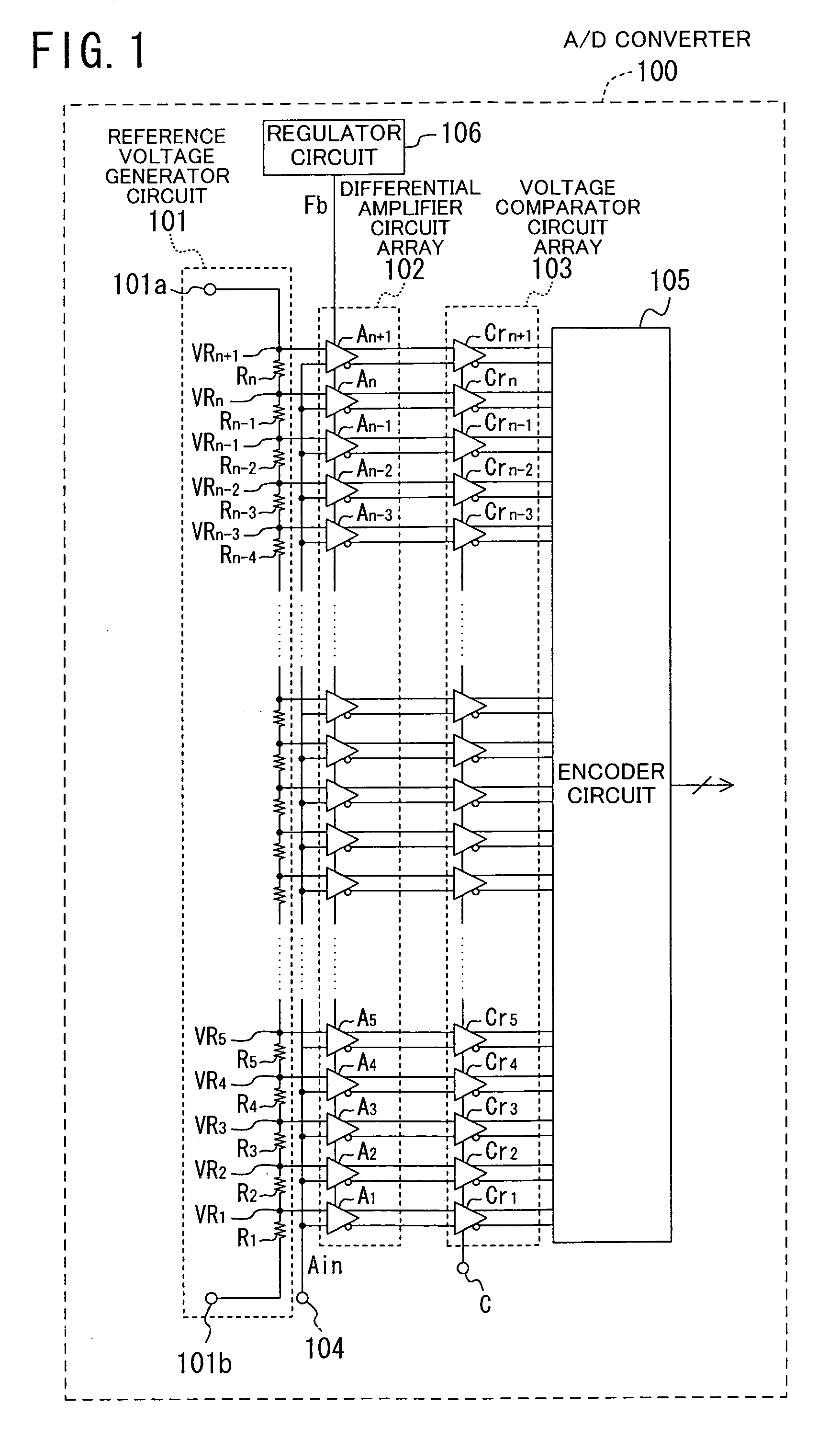
[0040]FIG. 1 is a circuit diagram illustrating the entire configuration of an A / D converter according to a first embodiment of the present invention.

[0041]In FIG. 1, an A / D converter 100 includes a reference voltage generator circuit 101, a differential amplifier circuit array 102, a voltage comparator circuit array 103, an encoder circuit (coding circuit) 105, and a regulator circuit 106.

[0042]The reference voltage generator circuit 101 generates a plurality (n+1) of reference voltages VR1 through VRn+1 by dividing a voltage between a high voltage side reference voltage applied to a high voltage side terminal 101a and a low voltage side reference voltage applied to a low voltage side terminal 101b by a plurality (n) of resistors R1 through Rn connected in series.

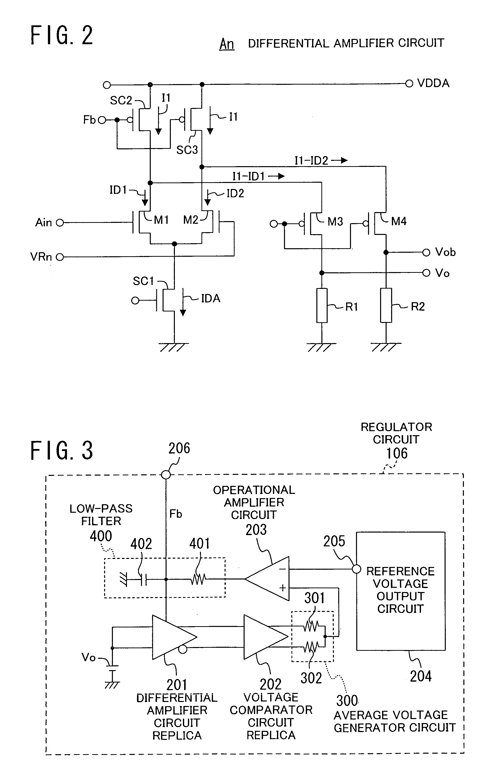
[0043]The generated reference voltages VR1 through VRn+1 are input to a differential amplifier circuit array 102. The differential amplifier circuit array 102 includes n+1 differential amplifier circuits A1 through An+1. Ea...

second embodiment

[0065]Next, an A / D converter according to a second embodiment of the present invention will be described with reference to FIG. 5.

[0066]FIG. 5 is a block diagram illustrating an exemplary arrangement of the voltage comparator circuits Cr1 through Crn+1 of the A / D converter 100 of FIG. 1. Each of the voltage comparator circuits Cr1 through Crn+1 has the same configuration and therefore the voltage comparator circuit Cr1 will be hereinafter described as an example.

[0067]The voltage comparator circuit Cr1 of FIG. 5 is a dynamic voltage comparator circuit characterized by its high-speed operation and low power consumption. The voltage comparator circuit Cr1 includes an input transistor section 10 with two NMOS transistors m1 and m2 and a positive feedback section 11 having a cross-couple inverter latch section with two NMOS transistors m3 and m4 and two PMOS transistors m7 and m8.

[0068]In the input transistor section 10, the two NMOS transistors m1 and m2 receive at their gates a non-in...

third embodiment

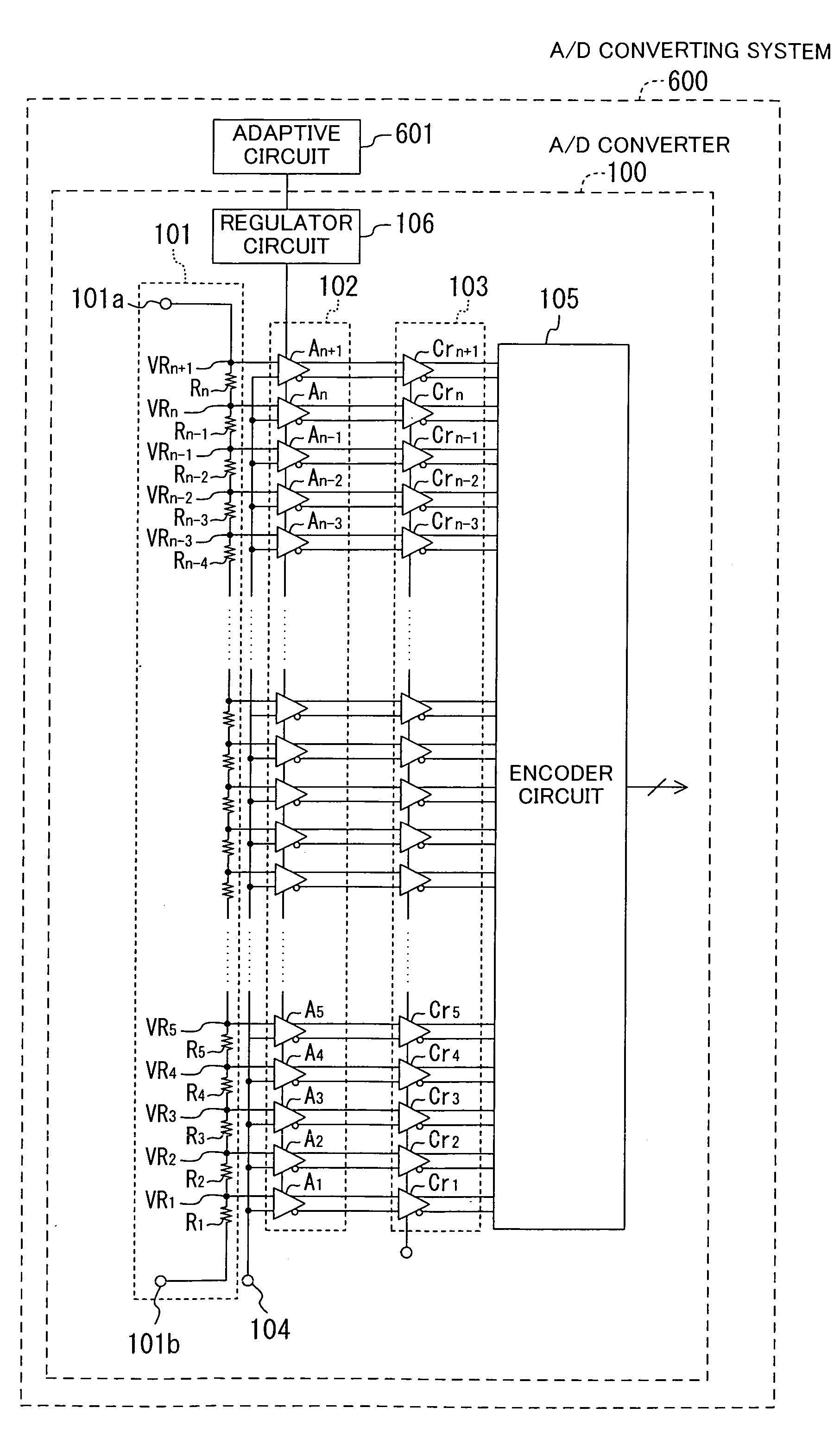
[0081]Next, an A / D converting system according to a third embodiment of the present invention will be described.

[0082]FIG. 10 is a diagram illustrating the entire configuration of an A / D converting system of this embodiment. An A / D converting system 600 of FIG. 10 includes an A / D converter 100 of FIG. 1 and an adaptive circuit 601 connected to the A / D converter 100.

[0083]The adoptive circuit 601 adaptively controls (leaning-controls) a predetermined reference voltage generated by the reference voltage output circuits 204 and 204′ (of FIGS. 4 and 5) built in the regulator circuit 601 of the A / D converter 100 of FIG. 1. Hereinafter, the internal configuration of the adaptive circuit 601 will be described. Note that as the voltage comparator circuits Cr1 through Crn+1 of the A / D converter 100, the dynamic voltage comparator circuit of FIG. 5 or FIG. 8 may be used, and also, for the voltage producing circuits 800a through 800n of the reference voltage output circuit 204′ of the regulato...


PUM


Abstract

In a flash A / D converter including a plurality of differential amplifier circuits and a plurality of voltage comparator circuits, a regulator circuit is provided. The regulator circuit automatically regulates a bias voltage of each of the plurality of differential amplifier circuits in a differential amplifier circuit array to make an output dynamic range for the differential amplifier circuits match an input dynamic range for the plurality of voltage comparator circuits. Therefore, even if the input dynamic range for the voltage comparator circuits is narrowed with reduction in a power supply voltage, the output dynamic range for the differential amplifier circuits and the input dynamic range for the voltage comparator circuits match, thus resulting in a high A / D conversion accuracy.

Description

CROSS REFERENCE TO RELATED APPLICATIONS[0001]This non-provisional application claims priority under 35 U.S.C. § 119(a) on patent application Ser. No. 2004-238094 filed in Japan on Aug. 18, 2004, the entire contents of which are hereby incorporated by reference.BACKGROUND OF THE INVENTION[0002]The present invention relates to A / D converters, and more particularly relates to a technique for suppressing degradation of A / D conversion characteristics due to changes in a power supply voltage, a surrounding temperature, properties of a semiconductor device or the like.[0003]FIG. 12 is a block diagram illustrating the configuration of a known A / D converter. The A / D converter of FIG. 12 is a full-flash type A / D converter and includes a reference voltage generator circuit 701, a differential amplifier circuit array 702, a voltage comparator circuit array 703, and an encoder circuit 705.[0004]The reference voltage generator circuit 701 generates a plurality of reference voltages VR1 through VR...

Claims


Application Information

Patent Timeline
Patent Type & Authority Patents(United States)
IPC IPC(8): H03M1/12
CPCH03M1/0604H03M1/365H03M1/0682
Inventor SUSHIHARA, KOJIMORIE, TAKASHI
Owner PANASONIC CORP
Why Eureka
Try Eureka