Multi-chip ball grid array package

a grid array and multi-chip technology, applied in the direction of electrical equipment, semiconductor devices, semiconductor/solid-state device details, etc., can solve the problems of increasing noise-like fluctuation and time distortion, reducing chip speed, and reducing switching noise, so as to improve signal propagation, reduce switching noise, and improve electronic characteristics

Inactive Publication Date: 2006-06-20
SAMSUNG ELECTRONICS CO LTD
View PDF17 Cites 21 Cited by
  • Summary
  • Abstract
  • Description
  • Claims
  • Application Information

AI Technical Summary

Benefits of technology

[0014]It is therefore an object of the present invention to provide a multi-chip BGA package that reduces switching noise, improves signal propagation, and generally improves electronic characteristics.

Problems solved by technology

For example, an increase in switching speed of the rerouted chip causes simultaneous switching noise due to fluctuation in chip power voltage.
This often decreases chip speed, increases noise-like fluctuation and time distortion, as well as increasing other operation errors.
Furthermore, when connecting a cable shield to a ground line, common-mode radiation occurs and serious electromagnetic interference (EMI) follows.
Additionally, complicated interconnection schemes in conventional multi-chip BGA packages increase parasitic inductance and deteriorate electric signal propagation.

Method used


Image

  • Multi-chip ball grid array package
  • Multi-chip ball grid array package
  • Multi-chip ball grid array package

Examples


first embodiment

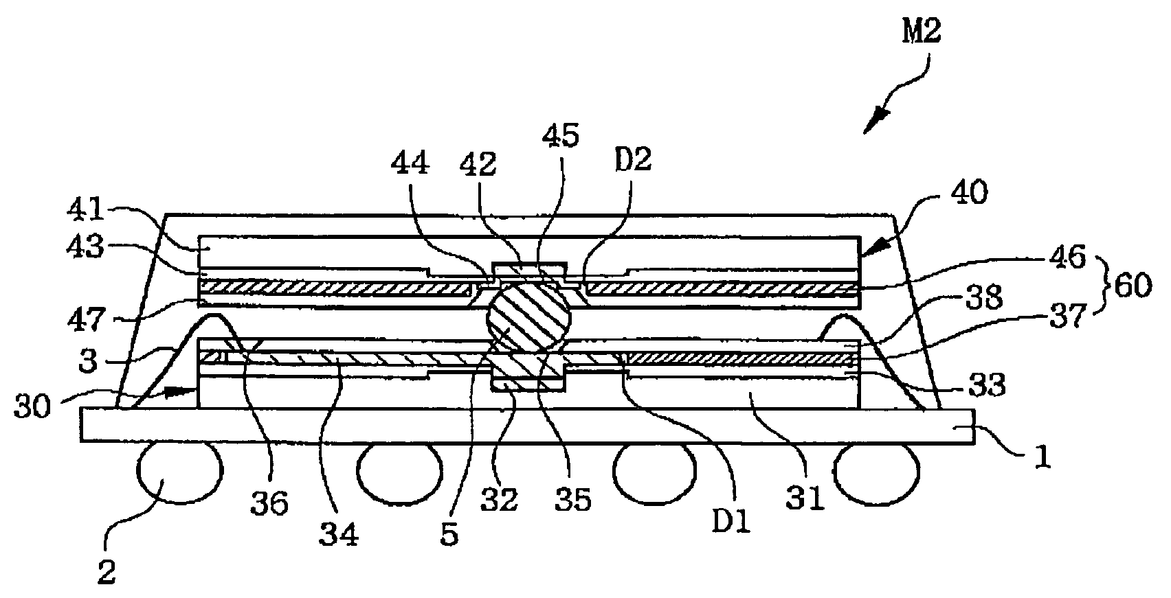
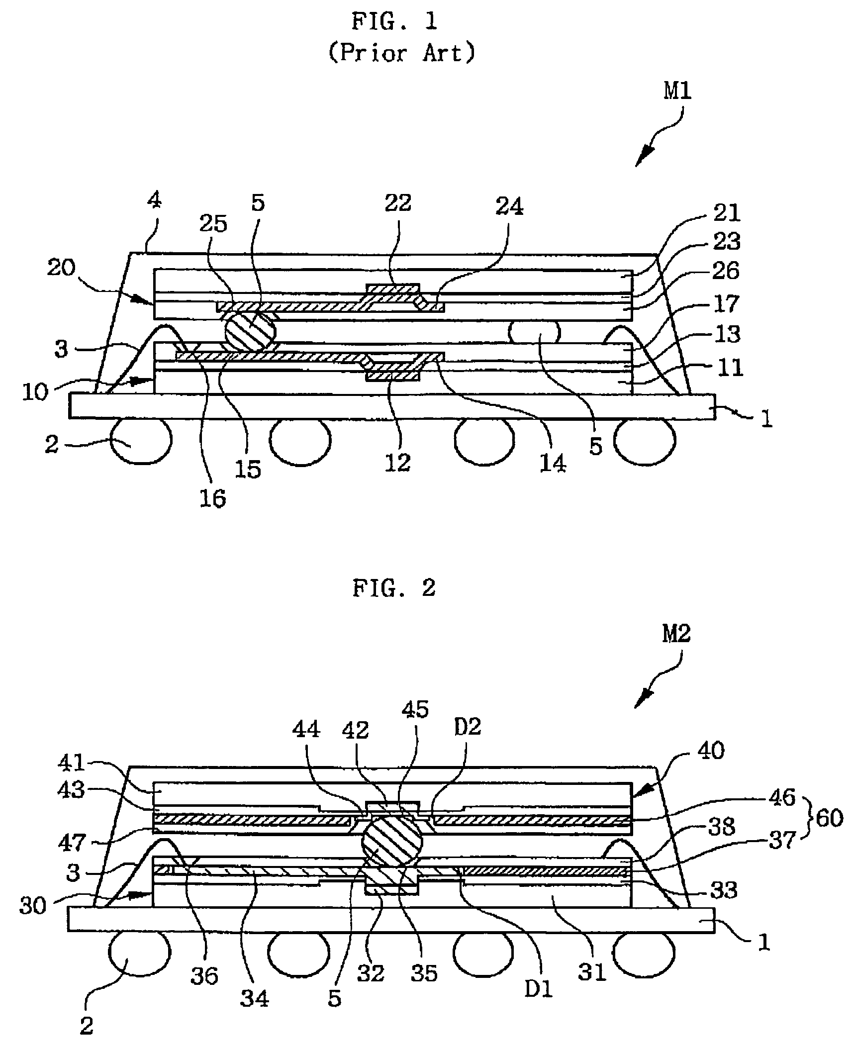
[0053]FIG. 2 schematically shows, in a cross-sectional view, a multi-chip BGA package M2 in accordance with a first embodiment of the present invention. As shown in FIG. 2, the multi-chip BGA package M2 includes first and second rerouted chips 30 and 40, first interconnection bump 5, a substrate 1, conductive balls 2, bonding wires 3, and an encapsulant 4.

[0054]Active surfaces of the first and second rerouted chips 30 and 40 face each other in a spaced arrangement.

[0055]The first rerouted chip 30 has a first semiconductor chip 31, a first insulating layer 33, first rerouting lines 34, a first electrode plate 37, and a second insulating layer 38.

[0056]The first semiconductor chip 31 is a center pad type. Specifically, the active surface of the first semiconductor chip 31 contains first chip pads 32 arranged centrally in a row. The first chip pads 32 protrude through a passivation layer (not shown) covering the active surface and made chiefly of silicon nitride. The first chip pads 32...

second embodiment

[0099]FIG. 4 schematically shows, in a cross-sectional view, a multi-chip BGA package M3 in accordance with a second embodiment of the present invention. The following description will not detail elements described previously, and will use the same reference numerals.

[0100]As shown in FIG. 4, the multi-chip BGA package M3 of this embodiment includes twentieth and third rerouted chips 40 and 100, the first interconnection bumps 5, the substrate 1, the conductive balls 2, the bonding wires 3, and the encapsulant 4.

[0101]The first interconnection bumps 5, the substrate 1, the conductive balls 2, the bonding wires 3, and the encapsulant 4 are substantially the same as described before in the first embodiment, respectively, so detailed descriptions about them are omitted. Furthermore, the twentieth rerouted chip 40 is similar to the aforementioned second rerouted chip, except that the second electrode plate 46 electrically connects with the ground pads of the second chip pads 42 and ther...

third embodiment

[0129]FIG. 6 schematically shows, in a cross-sectional view, a multi-chip BGA package M4 in accordance with a third embodiment of the present invention. In the following descriptions, some elements identical with the elements described earlier in the above first and second embodiments will not be described in detail, using the same reference numerals.

[0130]As shown in FIG. 6, the multi-chip BGA package M4 of this embodiment includes fourth and fifth rerouted chips 200 and 300, the first interconnection bumps 5, second interconnection bumps 6, the substrate 1, the conductive balls 2, the bonding wires 3, and the encapsulant 4.

[0131]The first interconnection bumps 5, the substrate 1, the conductive balls 2, the bonding wires 3, and the encapsulant 4 are similar to those described in the first embodiment, so detailed descriptions about them are omitted.

[0132]The fourth rerouted chip 200 includes third semiconductor chip 101, fifth insulating layer 103, first linking spots 104, third el...


PUM


Abstract

A multi-chip BGA package has two or more rerouted chips, each of which has one or more electrode plates. The electrode plate is coplanar with rerouting lines on the rerouted chip and may act as a decoupling capacitor, reducing simultaneous switching noise from fluctuations in power voltage, without causing an increase in thickness of the package. Further, each pair of rerouting lines on upper and lower rerouted chips includes two or more interconnection bumps. This reduces inductance and resistance of electric signal propagation. Therefore, the multi-chip BGA package of this invention can realize small, thin, high-speed and high-density memory devices.

Description

CROSS REFERENCE TO RELATED APPLICATIONS[0001]This U.S. non-provisional application claims priority under 35 U.S.C. § 119 to Korean Patent Application No. 2003-26581 filed Apr. 26, 2003, the contents of which are incorporated by reference.BACKGROUND OF THE INVENTION[0002]1. Field of the Invention[0003]The present invention relates generally to a multi-chip package with ball grid array (BGA), and more particularly, to a multi-chip BGA package with improved rerouting configuration for better signal propagation and decoupling capacitors for reduced switching noise.[0004]2. Description of the Related Art[0005]Multi-chip packaging involves mounting two or more chips on a lead frame or a circuit board. specifically, a BGA multi-chip package employs conductive balls arranged to provide electrical connections with external electronics.[0006]FIG. 1 shows an exemplary conventional multi-chip BGA package. Referring to FIG. 1, the multi-chip BGA package M1 includes lower and upper rerouted chips...

Claims


Application Information

Patent Timeline
Patent Type & Authority Patents(United States)
IPC IPC(8): H01L23/48H01L23/34H01L21/98H01L25/18H01L23/12H01L23/50H01L23/66H01L25/065H01L25/07
CPCH01L23/525H01L23/5286H01L23/66H01L25/0657H01L25/50H01L23/50H01L23/3128H01L2224/73207H01L24/10H01L2223/6627H01L2224/16145H01L2224/48091H01L2224/48227H01L2225/0651H01L2225/06513H01L2225/06524H01L2225/06527H01L2924/01078H01L2924/15311H01L2924/1903H01L2924/19033H01L2924/19041H01L2924/19104H01L2924/30107H01L2924/3011H01L2924/3025Y10S257/924H01L24/48H01L2924/00014H01L2924/12042H01L2224/05026H01L2224/05548H01L2224/05001H01L2224/05572H01L2224/05124H01L2224/05647H01L2224/05655H01L24/03H01L2224/02379H01L24/05H01L2924/00H01L2224/45099H01L2224/45015H01L2924/207H01L23/12
Inventor LEE, JONG-JOOLEE, DONG-HO
Owner SAMSUNG ELECTRONICS CO LTD
Why Eureka
Try Eureka