Non-volatile memory and method with bit line coupled compensation

a non-volatile memory and bit line coupled technology, applied in static storage, digital storage, instruments, etc., can solve the problems of unsuitable mobile and handheld environment, prone to mechanical failure, and bulky disk drives, and achieve high capacity, non-volatile memory devices of high performance, and disturbance effects inherent in high-density chip integration

Inactive Publication Date: 2006-06-20
SANDISK TECH LLC
View PDF49 Cites 103 Cited by
  • Summary
  • Abstract
  • Description
  • Claims
  • Application Information

AI Technical Summary

Benefits of technology

[0028]These needs for a high capacity and high performance non-volatile memory device are met by having a large page of read / write circuits to read and write a corresponding page of memory cells in parallel. In particular, disturbance effects inherent in high-density chip integration that may introduce errors into reading and programming are either eliminated or minimized.
[0029]When programming a contiguous page of storage units, every time a storage unit has reached its targeted state and is program-inhibited or locked out from further programming, it creates a perturbation on an adjacent storage unit still under programming. The present invention provides as part of a programming circuit and method in which an offset to the perturbation is added to the adjacent storage unit still under programming. The offset is added by a controlled coupling between the adjacent bit lines of the program-inhibited storage unit and the still under programming storage unit. In this way, an error inherent in programming in parallel high-density memory storage units is eliminated or minimized.
[0032]According to another aspect of the invention, the bit line of a storage unit still under programming is set to a potential that maximizes programming efficiency whenever both of its adjacent neighboring storage units are also still under programming. In the preferred embodiment, the bit line is set to the ground potential. This avoids any coupling from neighboring storage units who in turn may have their voltages boosted by adjacent storage unit under program inhibition.

Problems solved by technology

Conventional mass storage, based on rotating magnetic medium such as hard drives and floppy disks, is unsuitable for the mobile and handheld environment.
This is because disk drives tend to be bulky, are prone to mechanical failure and have high latency and high power requirements.
These undesirable attributes make disk-based storage impractical in most mobile and portable applications.
Programming of charge storage memory devices can only result in adding more charge to its charge storage elements.
This approach improves performances but does have repercussions on the accuracy of read and write operations.
Another issue has to do with bit line to bit line coupling or crosstalk.
This problem becomes more acute with parallel sensing of closely spaced bit lines.
However, the interleaving page architecture is disadvantageous in at least three respects.
First, it requires additional multiplexing circuitry.
Secondly, it is slow in performance.
Thirdly, it is also not optimum in addressing other disturb effects such as field coupling between neighboring charge storage elements at the floating gate level when the two neighbors are programmed at different times, such as separately in odd and even pages.
The problem of neighboring field coupling becomes more pronounced with ever closer spacing between memory transistors.
The conventional architecture of interleaving page exacerbates the error caused by neighboring charge storage unit coupling.
The read errors will become more severe with increasing density, requiring a more accurate read operation and wider partitioning of the threshold window for multi-state implementation.
Performance will suffer and the potential capacity in a multi-state implementation is limited.
This boosted voltage creates a significant perturbation on an adjacent storage unit still under programming.

Method used


Image

  • Non-volatile memory and method with bit line coupled compensation
  • Non-volatile memory and method with bit line coupled compensation
  • Non-volatile memory and method with bit line coupled compensation

Examples


first embodiment

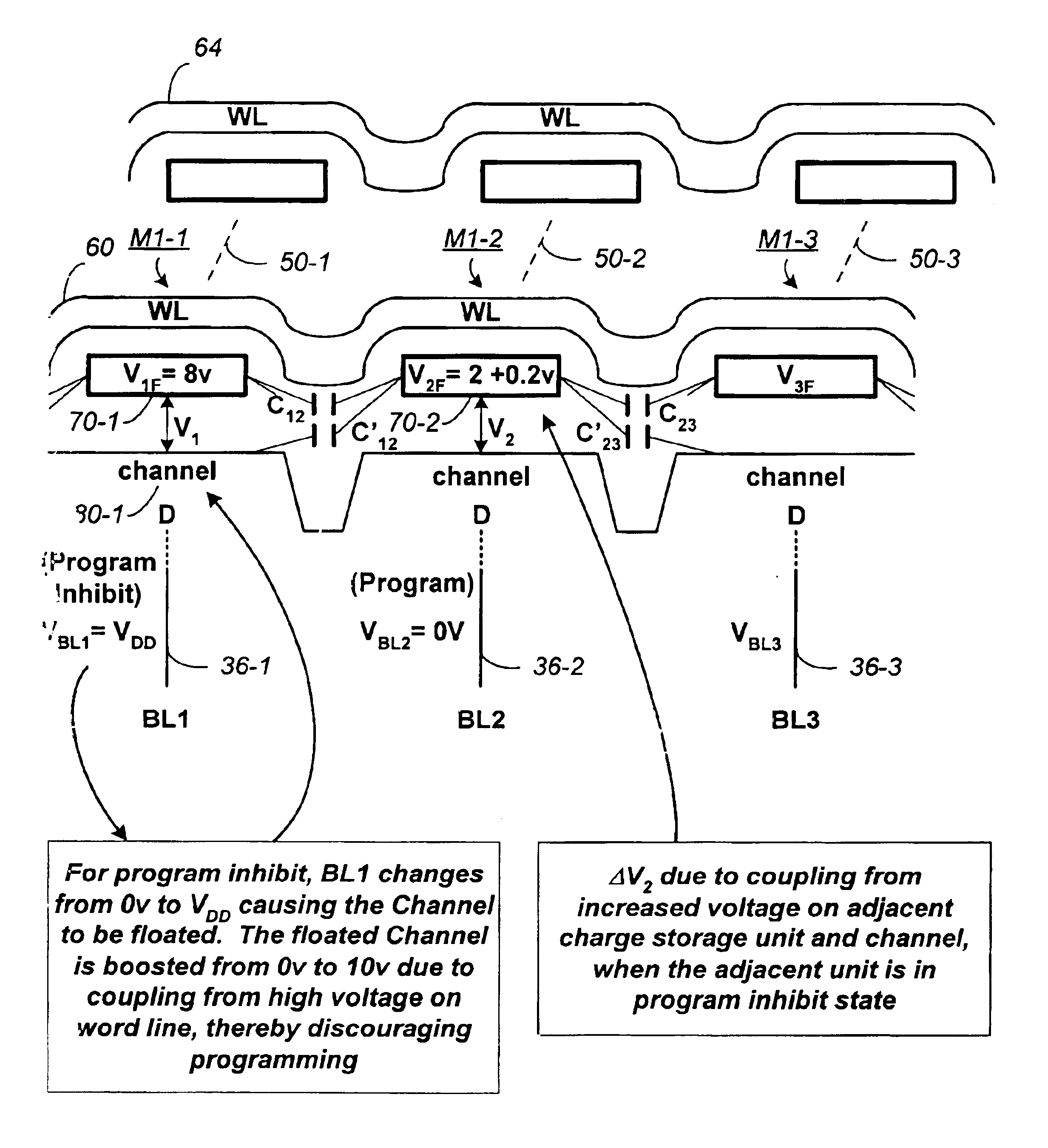
[0081]In the first embodiment just described, the second compensatory bit line boosting occurs before the first boosting. This provides a maximum range of possible ΔV1. On the other hand, it also means that the bit line of the memory transistor to be programmed will become floated and it voltage susceptible to be moved by subsequent high programming voltages. However, it has been estimated that the bit line capacitance is considerably greater than the channel capacitance, and therefore, even if the bit line is floated, the bit line and channel voltage will not change much when a high programming voltage appears on the control gate.

second embodiment

[0082]Alternatively, the first boosting is started first, followed by the second boosting. In this way, any coupling to the floated bit line due to high programming voltage is minimized.

[0083]FIGS. 9(A)-9(G) are timing diagrams illustrating the voltage compensation scheme by capacitive bit line-bit line coupling during program operations, according to a second embodiment of the invention.

Bit Lines Precharge & Boosting Phase:

[0084](1) The source select transistor is turned off by SGS at 0V (FIG. 9(A)) while the drain select transistor is turned on by SGD going high to VSG (FIG. 9(B)), thereby allowing a bit line to access a NAND chain.

[0085](2) The bit line voltage of a program inhibited NAND chain is raised (in the first of a two-step rise) to a predetermined voltage given by VDD−ΔV1 (FIG. 9(F)). This predetermined voltage is sufficient to cut off the drain of the NAND chain from its bit line when SGD drops to VDD in (3), thereby floating the channels therein. At the same time, the...


PUM


Abstract

When programming a contiguous page of memory storage units, every time a memory storage unit has reached its targeted state and is program-inhibited or locked out from further programming, it creates a perturbation on an adjacent memory storage unit still under programming. The present invention provides as part of a programming circuit and method in which an offset to the perturbation is added to the adjacent memory storage unit still under programming. The offset is added by a controlled coupling between the adjacent bit lines of the program-inhibited memory storage unit and the still under programming memory storage unit. In this way, an error inherent in programming in parallel high-density memory storage units is eliminated or minimized.

Description

FIELD OF THE INVENTION[0001]This invention relates generally to non-volatile semiconductor memory such as electrically erasable programmable read-only memory (EEPROM) and flash EEPROM, and specifically ones having improved programming and sensing circuits for a page of contiguous row of charge storage units.BACKGROUND OF THE INVENTION[0002]Solid-state memory capable of non-volatile storage of charge, particularly in the form of EEPROM and flash EEPROM packaged as a small form factor card, has recently become the storage of choice in a variety of mobile and handheld devices, notably information appliances and consumer electronics products. Unlike RAM (random access memory) that is also solid-state memory, flash memory is non-volatile, retaining its stored data even after power is turned off. In spite of the higher cost, flash memory is increasingly being used in mass storage applications. Conventional mass storage, based on rotating magnetic medium such as hard drives and floppy disk...

Claims


Application Information

Patent Timeline
Patent Type & Authority Patents(United States)
IPC IPC(8): G11C16/04G11C11/56G11C16/34
CPCG11C11/5628G11C11/5642G11C16/0483G11C16/3468G11C16/3418G11C16/3427G11C16/10G11C16/12G11C16/24
Inventor CERNEA, RAUL-ADRIANLI, YANMOFIDI, MEHRDADKHALID, SHAHZAD
Owner SANDISK TECH LLC
Why Eureka
Try Eureka