Fault detecting method and layout method for semiconductor integrated circuit

Inactive Publication Date: 2006-06-20
SOCIONEXT INC
View PDF17 Cites 11 Cited by
  • Summary
  • Abstract
  • Description
  • Claims
  • Application Information

AI Technical Summary

Benefits of technology

[0016]It is thus an object of the present invention to use physical information on a mask pattern in a chip of a semiconductor integrated circuit and the records of use of cells or functional blocks to enable accurate and efficient fault detections and layouts based on actual faults, thereby reducing faults such as initial defects.
[0018]The present invention thus enables accurate and efficient fault detections and layouts based on actual faults to reduce faults in the semiconductor integrated circuit such as initial defects.
[0031]The present invention thus uses the fault list corresponding to information on sites of the semiconductor integrated circuit where a fault is likely to occur, to perform detection for faults in the semiconductor integrated circuit, and uses the physical information on the mask pattern in the chip of the semiconductor integrated circuit and the records of use of cells or functional blocks to order and weight the faults with their likelihood. As a result, accurate and efficient fault detections and layouts are enabled based on actual faults, thereby reducing faults in the semiconductor integrated circuit such as initial defects.

Problems solved by technology

If, for example, fine foreign matter adheres to a mask in an integrated circuit manufacturing process, a defect such as a pattern bridge occurs in that portion to which the foreign matter adheres.
In an advanced integrated circuit, however, the number of test patterns executed is limited due to a limitation on a detection time associated with costs.
Due to a recent increase in the scale of integrated circuits, an enormous amount of test patterns and a large amount of processing time for fault simulation for the test patterns are required to obtain a high fault coverage.
An enormous amount of processing time is also required for the ATPG and a large amount of test patterns are automatically generated by the ATPG.
When a phenomenon that may cause a fault, for example, adhesion of foreign matter to a mask occurs in a physical area on a chip, this may lead to a fault if the foreign matter sticks to a portion where a mask pattern is present.
Typically, the mask pattern is not uniformly present on the chip; the mask pattern is dense in some areas, while it is coarse in the other areas.
Consequently, if a phenomenon that may cause a fault occurs substantially uniformly on the chip, the probability of an actual fault occurring is not uniform on the chip, but the fault occurrence rate is higher in dense portions in the mask pattern than in coarse portions in the mask pattern.
On contrary, portions with a high mask pattern density have a high fault occurrence rate with the same phenomenon that may cause a fault.
On the other hand, when, for example, a mask for a normal signal line is close to a mask for a power line, the integrated circuit is likely to malfunction due to a possible noise from a power supply.
If signal lines are close to each other, the integrated circuit is also likely to malfunction because a signal of a lower intensity is affected by a signal of a higher intensity.
Furthermore, the possibility of a fault occurring increases if a new process, a newly developed cell, or a cell or functional block the reliability of which has not been proved is used.
That is, fault simulation is carried out by assuming the possibility of an actual fault occurring for each fault to be subjected to detection to be constant, so that the conventional fault coverage may not be accurate enough to be an actual index of the fault occurrence rate.
In addition, the conventional fault detection is inefficient because it does not subject actually likely faults to the fault detection or the ATPG before less likely faults.
Additionally, due to the ever increasing scale and decreasing size of recent integrated circuits, there are expected to be new faults that cannot be expressed by the conventional single stuck-at fault model.
Furthermore, the conventional layout method does not take the likelihood of faults into consideration and takes no mask layout measures for preventing faults.

Method used


Image

  • Fault detecting method and layout method for semiconductor integrated circuit
  • Fault detecting method and layout method for semiconductor integrated circuit
  • Fault detecting method and layout method for semiconductor integrated circuit

Examples


first embodiment

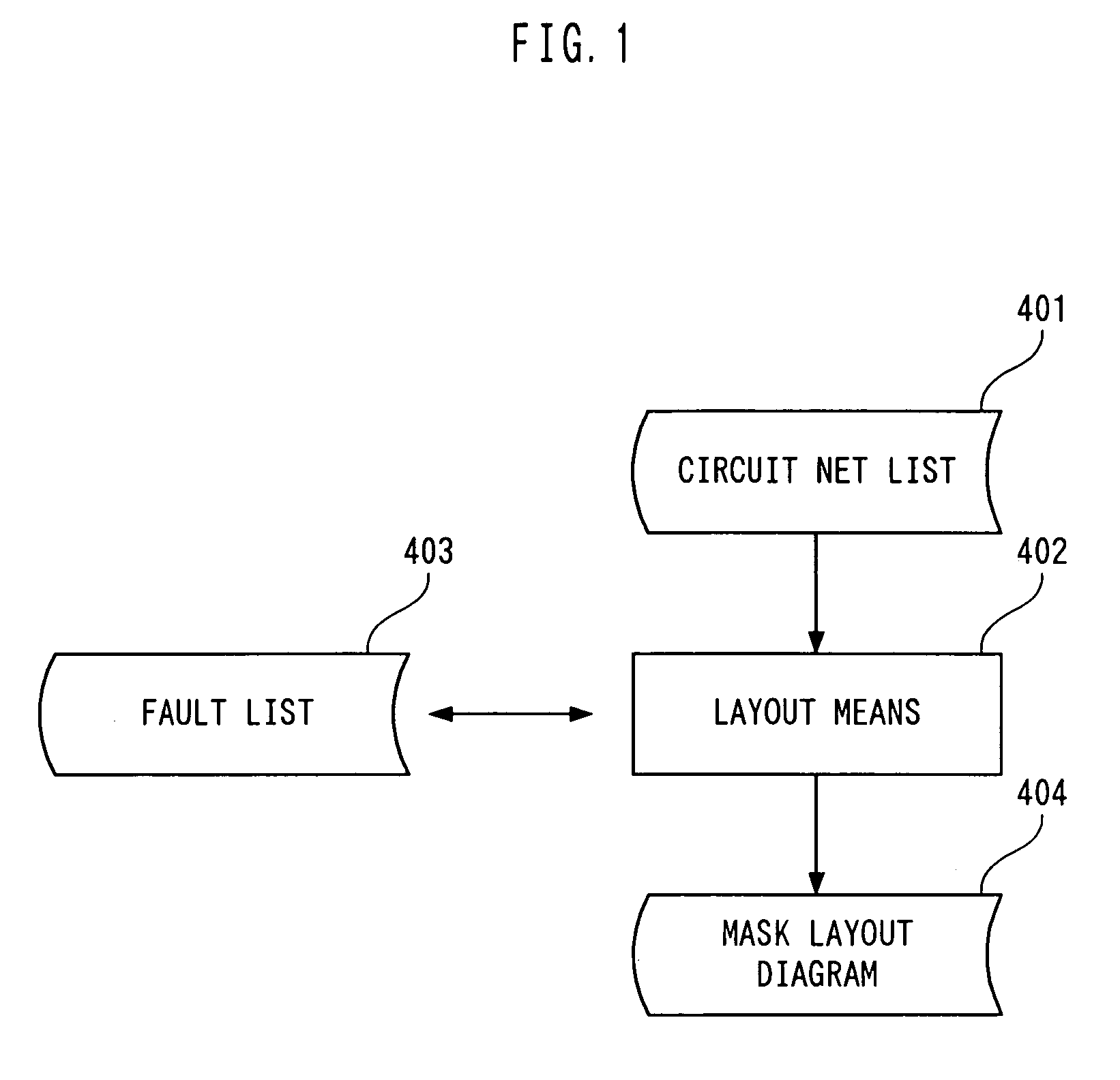
[0105]FIG. 1 is a diagram useful in explaining a Faults occurring in the integrated circuit vary depending on mask conditions, that is, the layout, wiring, and the type of the mask. They also vary depending on the level of records of use of cells and functional blocks in use. The fault occurrence rate of sites where a fault is likely to occur can be lowered by modifying the layout of the mask or the wiring. When, for example, a mask for a normal signal line is close to a mask for a power line, the integrated circuit is likely to malfunction due to a possible noise from a power supply. In this case, the possibility of a fault occurring can be reduced by increasing the interval between the power line and the mask.

[0106]In the prior art, a layout means 402 simply automatically generates a mask layout diagram 404 indicating the physical layout of a mask pattern or wiring for an integrated circuit based on a circuit netlist 401. According to the first embodiment of the present invention...

second embodiment

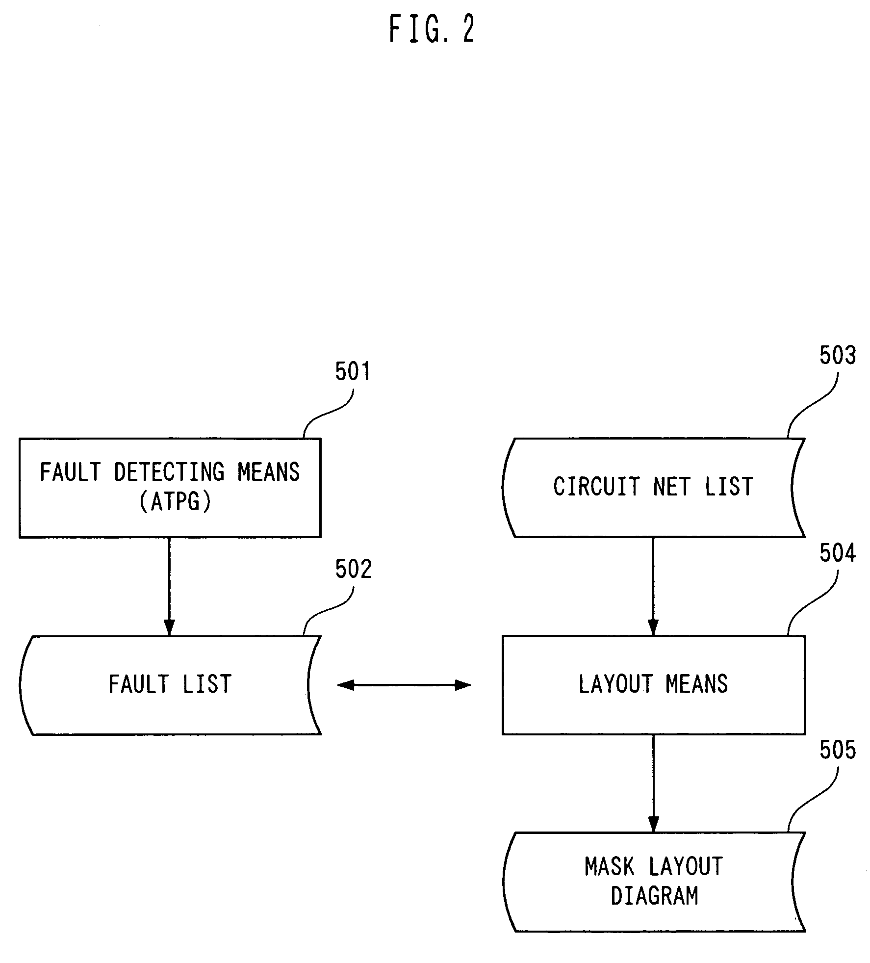
[0107]FIG. 2 is useful in explaining the present invention. In this embodiment, faults are detected to create a fault list. If the result of the fault detection indicates that there are faults undetected, new test patterns must be added. Once the fault coverage has increased to a certain level, an enormous amount of time is required to create test patterns to further increase the fault coverage and the test patterns involve a large number of steps. Even the ATPG may generate very long test patterns or may not automatically generate such test patterns. That is, it is difficult to achieve a fault coverage of 100% and in most cases, undetected faults remain. These undetected faults are missed even if they are occurring actually because there are no test patterns that can detect them. Certain measures must be taken to minimize the occurrence of such faults.

[0108]Thus, according to the second embodiment, a fault list 502 output from a fault detecting means 501 is loaded in a layout means...

third embodiment

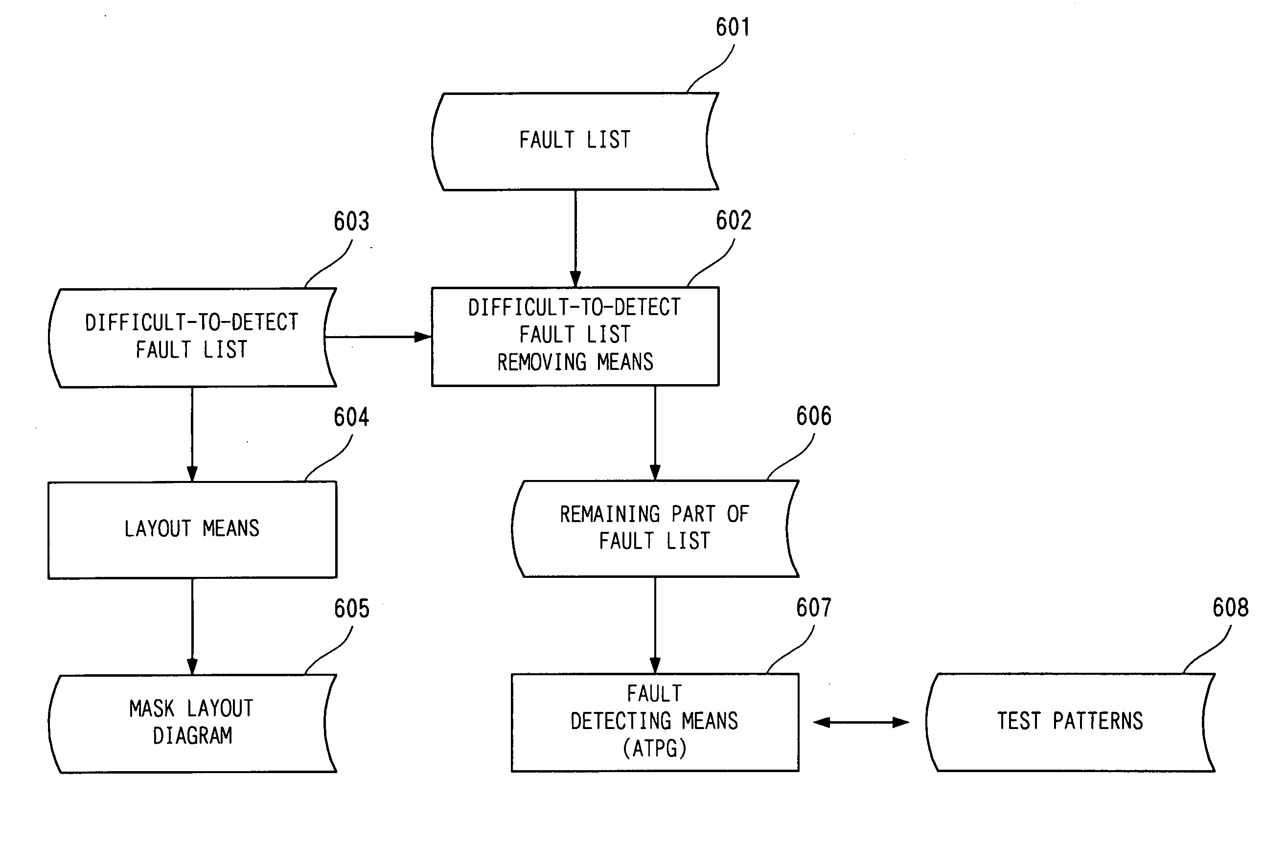
[0110]FIG. 3 is useful in explaining the present invention. One of the reasons why a large amount of processing time is required for the fault detection is faults that are difficult to detect or cannot be detected.

[0111]In the fault detection, the detection time required to detect each fault is not uniform and varies significantly depending on how easily the fault is detected or the amount of events occurring during the detection. If a large amount of events occur during the detection, the load on hardware for a fault detector increases the amount of processing time. The fault detection is more effective when test patterns that are more likely to be detected or faults that can be more easily detected are processed before faults that require a larger amount of processing time due to events or when another measures are taken without processing the latter faults.

[0112]Some of the faults in the circuit that are difficult to detect are known. For example, flipflop pins on scan lines in a...


PUM


Abstract

The present invention provides a fault detecting method and a layout method for a semiconductor integrated circuit. The fault detecting method performs detection for faults in a semiconductor integrated circuit using a fault list corresponding to information on sites in the semiconductor integrated circuit where a fault is likely to occur or information required to reduce such faults. In addition, the fault detecting method and the layout method perform ordering of faults with their likelihood and weighting of the faults, taking into consideration physical information on a mask pattern within a chip or records of actual use of cells or functional blocks.

Description

FIELD OF THE INVENTION[0001]The present invention relates to a fault detecting method and a layout method for a semiconductor integrated circuit, and in particular, to a fault detecting method and a layout method for a semiconductor integrated circuit which can efficiently and accurately perform detection for faults in a semiconductor integrated circuit and lay it out, respectively.BACKGROUND OF THE INVENTION[0002]In a conventional layout process for a mask pattern for a semiconductor integrated circuit, a layout device automatically generates a mask layout diagram indicating the physical layout of a mask pattern or wiring for an integrated circuit based on a logically verified circuit netlist. Since a circuit diagram has no practical physical information, the physical positional relationship in the mask pattern are given only through the layout process. In most cases, the physical positions of the mask pattern in the layout are based on timing information on logical operations of t...

Claims


Application Information

Patent Timeline
IPC IPC(8): G01R31/28G01R31/3183G06F17/50H01L21/66H01L21/82
CPCG01R31/2846G06F17/5081G01R31/31835G06F2217/12G06F30/398G06F2119/18Y02P90/02H01L22/00
Inventor YOSHIDA, TAKAKISHIMODA, REISUKE
Owner SOCIONEXT INC
Why Eureka
Try Eureka