

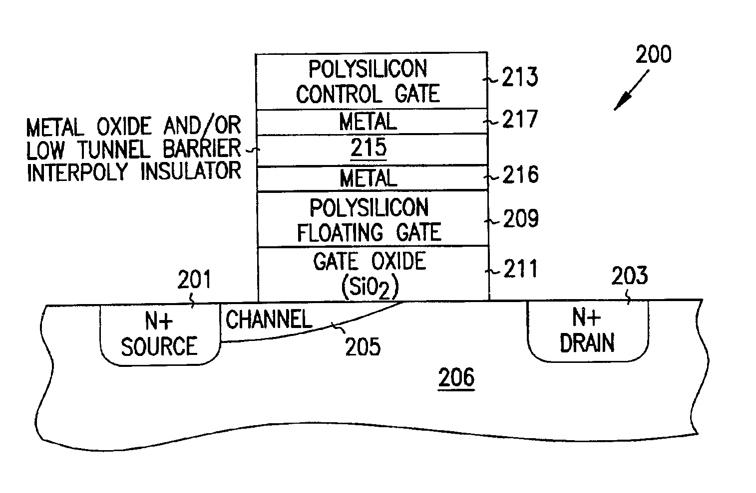
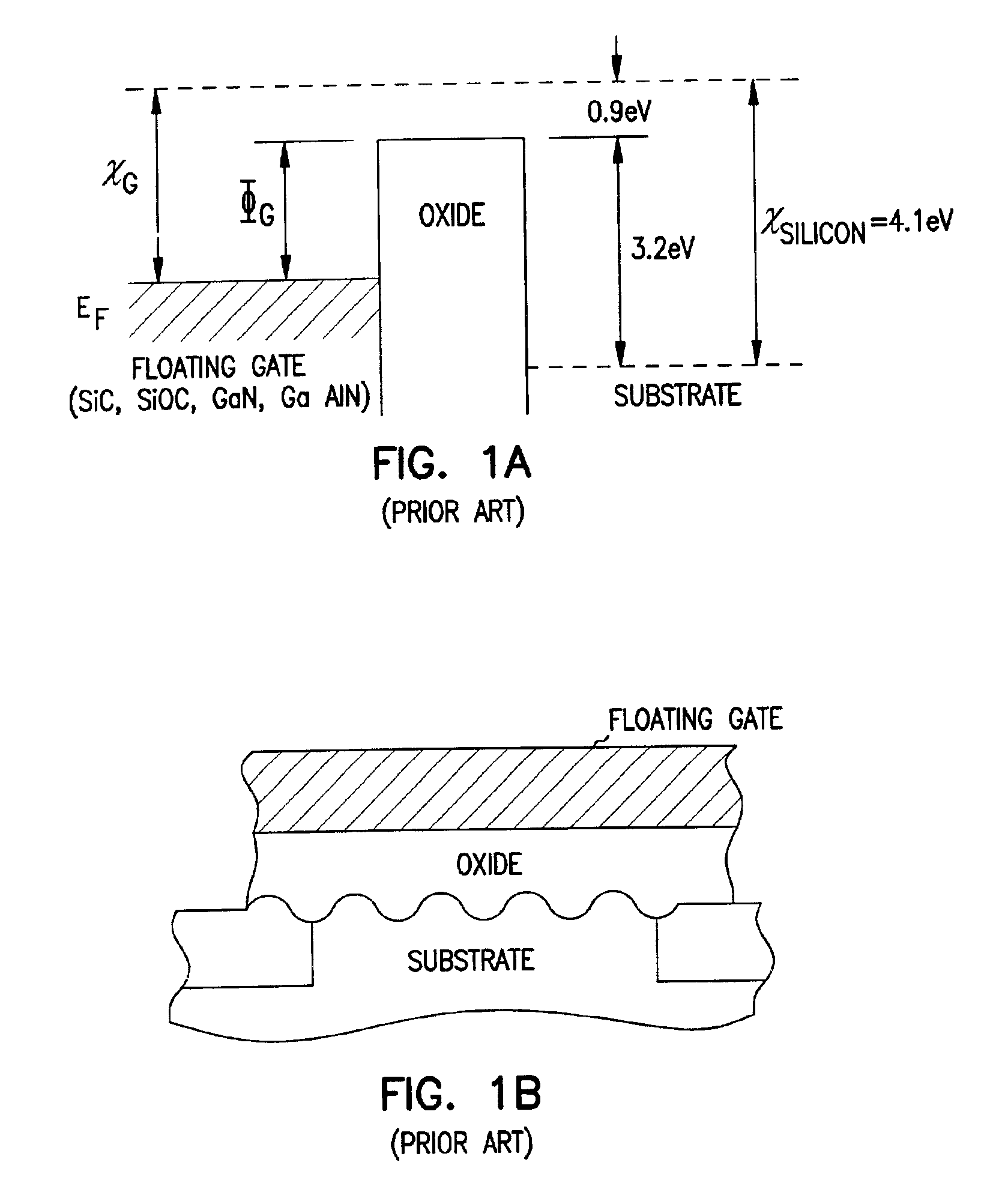
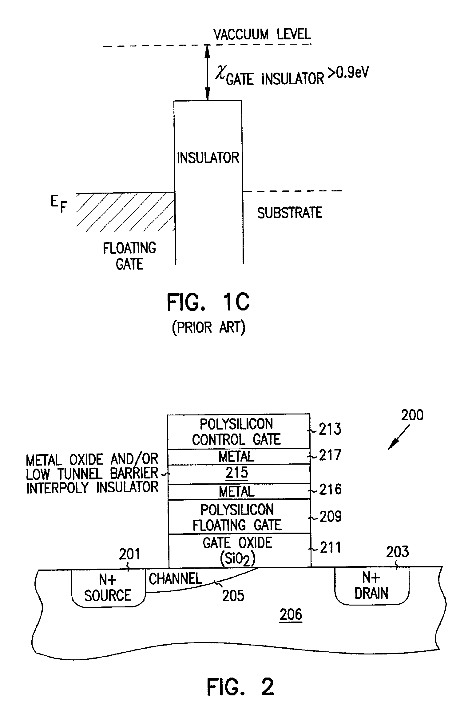
Flash memory with low tunnel barrier interpoly insulators
a technology of interpoly insulators and flash memory, which is applied in the field of integrated circuits, can solve the problems of premature breakdown and reliability problems, poor quality of interpoly oxides, and localized high electric fields
- Summary
- Abstract
- Description
- Claims
- Application Information
AI Technical Summary
Benefits of technology
Problems solved by technology
Method used
Image

Examples
example i
Formation of PbO Tunnel Barriers
[0076]This oxide barrier has been studied in detail using Pb / PbO / Pb structures. The oxide itself can be grown very controllably on deposited lead films using either thermal oxidation (see generally, J. M. Eldridge and J. Matisoo, “Measurement of tunnel current density in a Meal-Oxide-Metal system as a function of oxide thickness,” Proc. 12th Intern. Conf. on Low Temperature Physics, pp. 427-428, 1971; J. M. Eldridge and D. W. Dong, “Growth of thin PbO layers on lead films. I. Experiment,” Surface Science, Vol. 40, pp. 512-530, 1973) or rf sputter etching in an oxygen plasma (see generally, J. H. Greiner, “Oxidation of lead films by rf sputter etching in an oxygen plasma”, J. Appl. Phys., Vol. 45, No. 1, pp. 32-37, 1974). It will be seen that there are a number of possible variations on this structure. Starting with a clean poly-Si substrate, one processing sequence using thermal oxidation involves:
[0077](i) Depositing a clean lead film on the poly-Si ...
example ii
Formation of Al2O3 Tunnel Barriers
[0082]A number of studies have dealt with electron tunneling in Al / Al2O3 / Al structures where the oxide was grown by “low temperature oxidation” in either molecular or plasma oxygen (see generally, S. M. Sze, Physics of Semiconductor Devices, Wiley, N.Y., pp. 553-556, 1981; G. Simmons and A. El-Badry, “Generalized formula for the electric tunnel effect between similar electrodes separated by a thin insulating film,” J. Appl. Phys., Vol. 34, p. 1793, 1963; S. R. Pollack and C. E. Morris, “Tunneling through gaseous oxidized films of Al2O3,” Trans. AIME, Vol. 233, p. 497, 1965; Z. Hurych, “Influence of nonuniform thickness of dielectric layers on capacitance and tunnel currents,” Solid-State Electronics, Vol. 9, p. 967, 1966; S. P. S. Arya and H. P. Singh, “Conduction properties of thin Al2O3 films,” Thin Solid Films, Vol. 91, No. 4, pp. 363-374, May 1982; K.-H. Gundlach and J. Holzl, “Logarithmic conductivity of Al—Al2O3—Al tunneling junctions produced...
example iii
Formation of Single- and Multi-Layer Transition Metal Oxide Tunnel Barriers
[0090]Single layers of Ta2O5, TiO2, ZrO2, Nb2O5 and similar transition metal oxides can be formed by “low temperature oxidation” of numerous Transition Metal (e.g., TM oxides) films in molecular and plasma oxygen and also by rf sputtering in an oxygen plasma. The thermal oxidation kinetics of these metals have been studied for decades with numerous descriptions and references to be found in the book by Kubaschewski and Hopkins (O. Kubaschewski and B. E. Hopkins, “Oxidation of Metals and Alloys”, Butterworth, London, pp. 53-64, 1962). In essence, such metals oxidize via logarithmic kinetics to reach thicknesses of a few to several tens of angstroms in the range of 100 to 300C. Excellent oxide barriers for Josephson tunnel devices can be formed by rf sputter etching these metals in an oxygen plasma (see generally, J. M. Greiner, “Josephson tunneling barriers by rf sputter etching in an oxygen plasma,” J. Appl. ...
PUM
 Abstract
Description
Claims
Application Information