InP-based photonic integrated circuits with Al-containing waveguide cores and InP-based array waveguide gratings (AWGs) and avalanche photodiodes (APDs) and other optical components containing an InAlGaAs waveguide core

a photonic integrated circuit and waveguide core technology, applied in the field of active and passive devices of semiconductors, can solve problems such as affecting performance and yield, and affecting the performance and yield of inp-based awgs

Inactive Publication Date: 2006-07-04
INFINERA CORP
View PDF32 Cites 30 Cited by
  • Summary
  • Abstract
  • Description
  • Claims
  • Application Information

AI Technical Summary

Benefits of technology

[0011]According to this invention, the performance and yield of InP-based optical components, such as array waveguide gratings (AWGs) and avalanche photodiodes (APDs) is greatly improved by replacing the InGaAsP waveguide generally present in these InGaAsP / InP devices with an Al-containing quaternary, InAlGaAs waveguide. InAlGaAs is superior to InGaAsP in the case of both reduced compositional quaternary variations as evidenced by photoluminescent (PL) emission wavelength variations across the wafer as well as higher run-to-run reproducibility in a MOCVD reactor. The deployment of InAlGaAs waveguides provides for high uniform photoluminescent (PL) emission wavelength across the wafer for InAlGaAs waveguides as compared to InGaAsP waveguides as now commonly employed in such optical devices or components. For example, typical variation of PL wavelength across a 2 inch wafer for InAlGaAs is less than 2 nm which is dramatically much less than that for InGaAsP across a 2 inch wafer which is in the range of approximately 10 nm to 20 nm. As a result, the performance and yield of optical components is significantly improved for devices that utilize InAlGaAs instead of InGaAsP as the basic waveguide or core material in the device or circuit waveguide. Note that any waveguide or core structure that currently employs InGaAsP can be transformed, via this invention, to InAlGaAs whether a discrete component or multiple optically coupled components formed in photonic integrated circuits (PIC).
[0013]In another feature of this invention, a non-Al-containing layer is directly deposited on the InAlGaAs waveguide core or layer formed in an InP-based semiconductor device to bury the Al-containing waveguide or core layer, protecting it from subsequent oxidation and degradation, particularly during subsequent epitaxial regrowth or heat treatment processes.

Problems solved by technology

An InGaAsP waveguide core is problematic due to the fact that significant composition variations occur across the wafer as the material is grown epitaxially, which is typically via a MOCVD reactor.
These composition variations wreak havoc on the performance and yield of InP-based AWGs and other optical components that utilize InGaAsP as the core waveguide layer.
Furthermore, InGaAsP materials can also be difficult to target (reproducibility) from one epitaxial growth to the next, further affecting performance and yield.
However, there is no teaching or appreciation in the art of utilizing InAlGaAs waveguide structures in photonic integrated circuits (PICs) where high wavelength uniformity is required, necessary and achieved across the wafer when deploying InAlGaAs in lieu of InGaAsP as the waveguide or core for the optical coupling path among plural active and passive optical components integrated in the PIC.

Method used


Image

  • InP-based photonic integrated circuits with Al-containing waveguide cores and InP-based array waveguide gratings (AWGs) and avalanche photodiodes (APDs) and other optical components containing an InAlGaAs waveguide core
  • InP-based photonic integrated circuits with Al-containing waveguide cores and InP-based array waveguide gratings (AWGs) and avalanche photodiodes (APDs) and other optical components containing an InAlGaAs waveguide core
  • InP-based photonic integrated circuits with Al-containing waveguide cores and InP-based array waveguide gratings (AWGs) and avalanche photodiodes (APDs) and other optical components containing an InAlGaAs waveguide core

Examples


Embodiment Construction

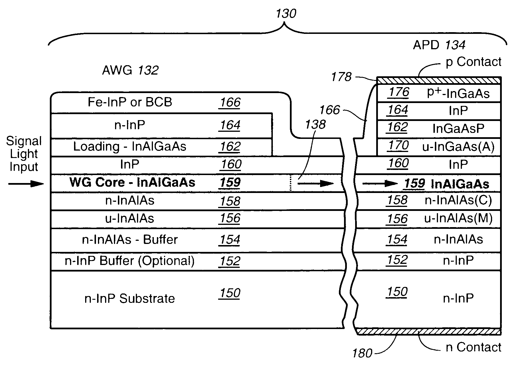
[0033]As used herein, the term, “waveguide” is also an optical waveguide core or material as well as any other optical waveguide in a semiconductor Group III–V as-grown structure or device. In the case of waveguide cores, the core can be continuous and co-planar or stepped and non-planar from one optical component to another among one or more optical components in a photonic integrated circuit (PIC).

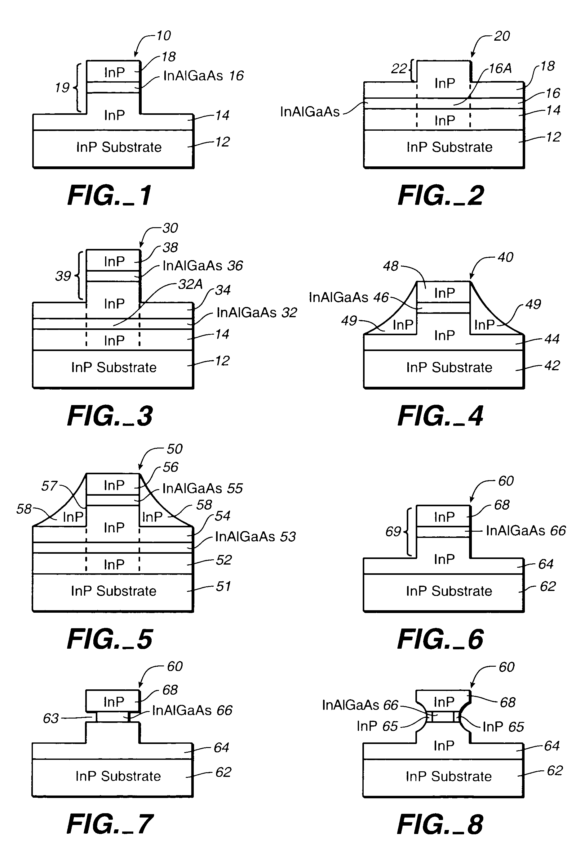
[0034]Reference now is made to FIGS. 1–5 for examples of semiconductor structures that may utilize an InAlGaAs quaternary compound as a waveguide or core in accordance with this invention. The semiconductor structures shown in FIGS. 1–5 are, therefore, exemplary of the deployment of this invention.

[0035]Also, as used herein, an optical combiner may be comprised of a power coupler, star coupler, a MMI coupler, an Echelle grating or an arrayed waveguide grating (AWG). To be noted is that there is an absence in the art, at least to the present knowledge of the inventors herein, of the teach...


PUM


Abstract

The Group III–V quaternary, InAlGaAs is employed as a waveguide layer in optical components, such as In-P based array waveguide gratings (AWGs), avalanche photodiodes (APDs) or other optical components that contain a waveguide core in the InP regime. The deployment of InAlGaAs waveguides provides for high uniform photoluminescent (PL) emission wavelength across the wafer for InAlGaAs waveguides as compared to InGaAsP waveguides as now commonly employed in such optical devices or components. The use of an InAlGaAs waveguide core has particular utility when deployed in a photonic integrated circuit (PIC) such as an AWG with a plurality of outputs optically integrated with a plurality of photodetectors, such as APDs which are exemplified in this disclosure. In lieu of an InAlGaAs waveguide, combination layers of InGaAs / InAlAs, InGaAs / InAlGaAs or InAlAs / InAlGaAs may be employed or stacks of such layers to form the waveguides in the PIC chip.

Description

REFERENCE TO RELATED APPLICATION[0001]This application claims priority of provisional application, Ser. No. 60 / 342,984, filed Dec. 21, 2001, which provisional application is incorporated herein by its reference, and this application is a continuation-in-part of nonprovisional patent applications, Ser. No. 10 / 267,331, filed Oct. 8, 2002 and entitled, TRANSMITTER PHOTONIC INTEGRATED CIRCUITS (TxPIC) AND OPTICAL TRANSPORT NETWORKS EMPLOYING TxPICs; and Ser. No. 10 / 267,304, filed Oct. 8, 2002; and entitled, AN OPTICAL SIGNAL RECEIVER PHOTONIC INTEGRATED CIRCUIT (RxPIC), AN ASSOCIATED OPTICAL SIGNAL TRANSMITTER PHOTONIC INTEGRATED CIRCUIT (TxPIC) AND AN OPTICAL TRANSPORT NETWORK UTILIZING THESE CIRCUITS, which nonprovisional patent applications are incorporated herein by their reference.BACKGROUND OF THE INVENTION[0002]1. Field of the Invention[0003]This invention relates generally to semiconductor active and passive devices, such as photonic, electronic or optoelectronic devices or arra...

Claims


Application Information

Patent Timeline
Patent Type & Authority Patents(United States)
IPC IPC(8): G02B6/00G02B6/10G02B6/12
CPCG02B6/12004G02B6/12011G02B6/12019H01S5/0268G02B6/131H01S5/4031G02B2006/12078H01S5/026
Inventor NAGARAJAN, RADHAKRISHNAN L.DENTAI, ANDREW G.KISH, JR., FRED A.
Owner INFINERA CORP
Why Eureka
Try Eureka