Low voltage EEPROM memory arrays

a memory array and low voltage technology, applied in the field of eeprom memory cells and memory arrays, can solve the problems of high current, difficult to reduce the cell size of memory cells, high power consumption for operation, etc., and achieve the effect of increasing the cell read current of the memory array

Inactive Publication Date: 2006-07-11
SPADEA GREGORIO
View PDF9 Cites 49 Cited by
  • Summary
  • Abstract
  • Description
  • Claims
  • Application Information

AI Technical Summary

Benefits of technology

[0012]According to one aspect of the present invention, a non-volatile memory array includes memory cells formed in columns of isolated well regions and connected in a common source arrangement so that Fowler-Nordheim (FN) tunneling is used for both program (write) and erase operations of the memory cells. According to another aspect of the present invention a group of memory cells can be connected in series as it is done in NAND arrays but such array can be used as a byte alterable EEPROM with parallel access as a conventional NOR array. Furthermore, in another embodiment, an insulated gate bipolar transistor (IGBT) is coupled to the memory cells to increase the cell read current of the memory array. When the memory array incorporates IGBTs on the bitlines, the cell read current becomes independent of the wordline voltages. Thus, the memory array of the present invention can be operated at lower voltages than in the case when such IGBT is not present. The use of the IGBTs in the memory array of the present invention enables formation of embedded non-volatile memories in digital integrated circuits which operate from power supply voltages as low as 1.0 Volt.

Problems solved by technology

First, one class of conventional non-volatile memories often employ channel hot electron injection for program (write), thereby requiring a high current and, consequently, high power consumption for the operation.
The use of two vertical metal lines makes it difficult to reduce the cell size of the memory cells.
Another problem common to non-volatile memory cells based on the floating gate concept is the formation of the control gate.
For the small feature size technologies, a second problem is created by the height of the stack made with the floating gate and the control gate in a stack gate arrangement which could be excessive and could create potential shorts to the first level of metal.
In addition, for the self-aligned stacked gate cell, the gate coupling ratio (the ratio of the capacitance between the floating gate and the control gate and the total capacitance of the floating gate) cannot be easily increased without increasing the size of the cell.
Another common problem encountered in conventional non-volatile memory arrays is the amount of cell current which can be obtained from the memory cell during read.

Method used


Image

  • Low voltage EEPROM memory arrays
  • Low voltage EEPROM memory arrays
  • Low voltage EEPROM memory arrays

Examples


Embodiment Construction

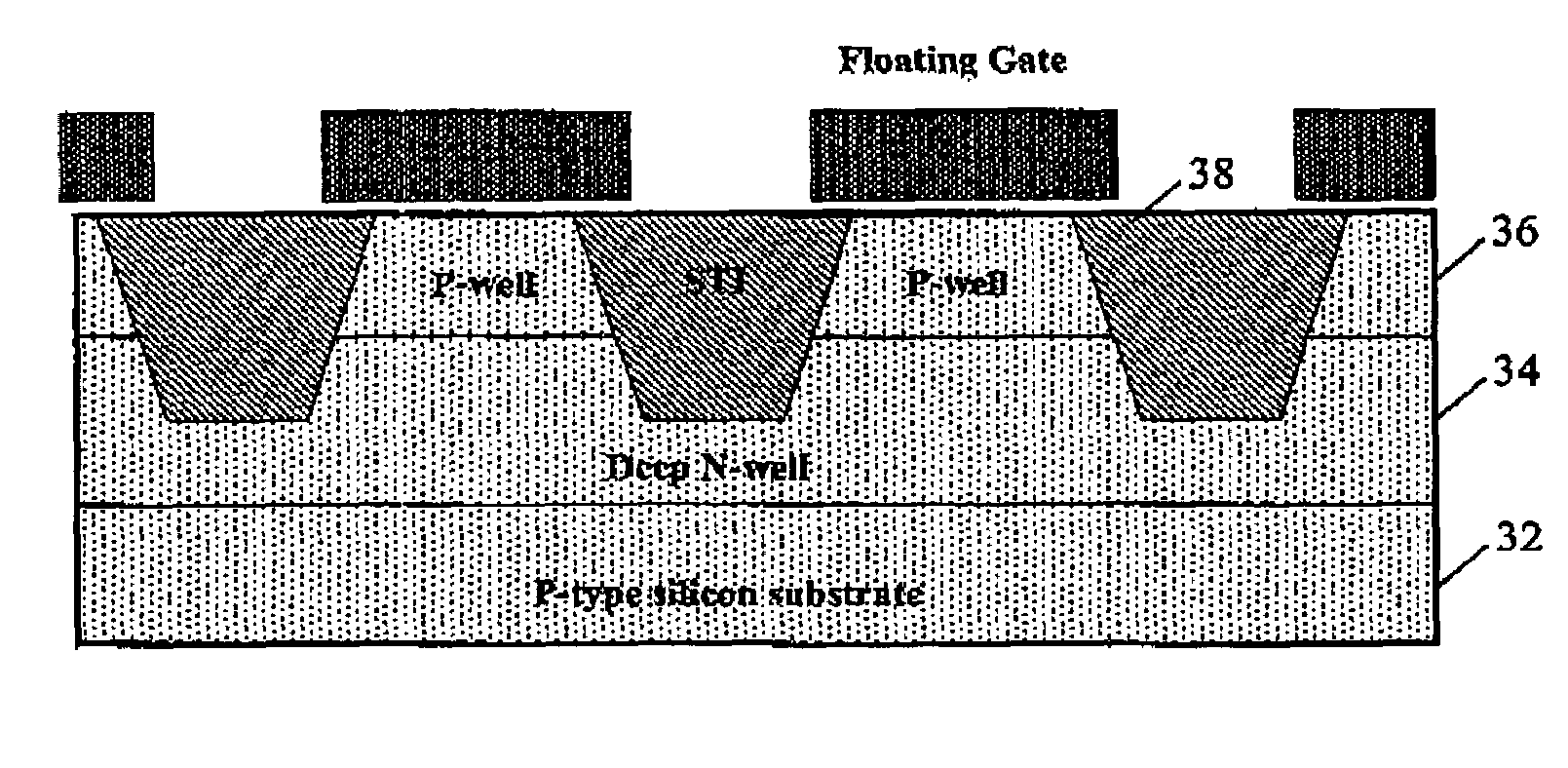
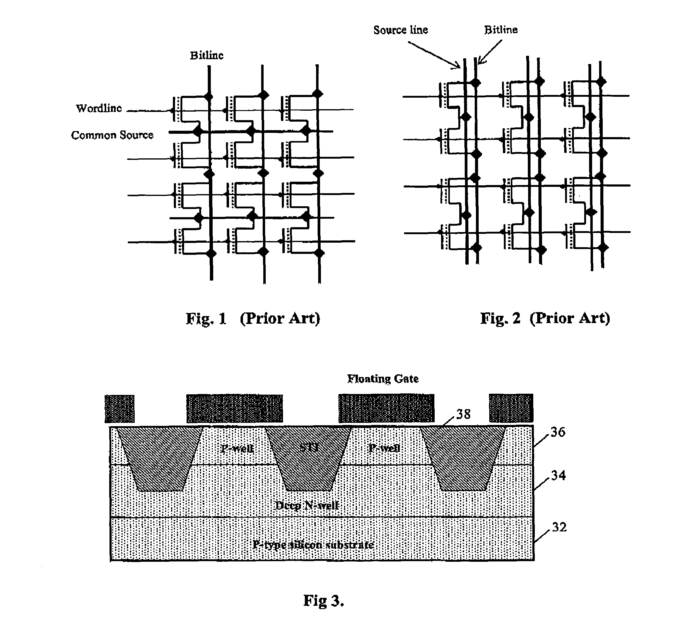
[0053]In accordance with the principles of the present invention, a non-volatile memory array includes memory cells formed in columns of isolated well regions and connected in a common source arrangement so that Fowler-Nordheim (FN) tunneling is used for both program (write) and erase operations of the memory cells. In one embodiment, the memory array of the present invention is formed as a byte alterable EEPROM with parallel access. More specifically, writing of the EEPROM is carried out on each byte while erasing of the EEPROM is carried out selectively on each bit of memory cells. In one embodiment, the memory array of the present invention is formed using NMOS transistors in P-wells isolated by shallow trench isolation. The memory array of the present invention can be formed as a common source NOR array or a common source NAND array. In one embodiment, an insulated gate bipolar transistor (IGBT) is coupled to the memory cells to increase the cell read current of the memory array...


PUM


Abstract

A non-volatile memory array includes memory cells connected in a common source arrangement and formed in columns of isolated well regions so that Fowler-Nordheim tunneling is used for both write and erase operations of the memory cells. The memory arrays can be formed as NOR arrays or NAND arrays. In one embodiment, the memory array of the present invention is formed as a byte alterable EEPROM with parallel access. In another embodiment, an insulated gate bipolar transistor (IGBT) is coupled to the memory cells to increase the cell read current of the memory array. When the memory array incorporates IGBTs on the bitlines, the cell read current becomes independent of the wordline voltages. Thus, the memory array of the present invention can be operated at low voltages. The use of IGBTs in the memory array of the present invention enables formation of embedded non-volatile memories in low-voltage digital integrated circuits.

Description

CROSS-REFERENCE TO RELATED APPLICATIONS[0001]This application claims the benefit of U.S. Provisional Patent Application Ser. No. 60 / 525,580, filed on Nov. 26, 2003, having the same inventorship hereof, which application is incorporated herein by reference in its entirety.FIELD OF THE INVENTION[0002]The invention relates to semiconductor non-volatile memories and, in particular, to EEPROM memory cells and memory arrays capable of write and erase operations with low power consumption.DESCRIPTION OF THE RELATED ART[0003]Non-volatile memory devices and electrically erasable programmable read only memory (EEPROM) devices are known. In many applications, it is desirable to embed non-volatile memory blocks into low voltage digital integrated circuits. The technology for manufacturing low voltage digital integrated circuits is well established in the industry. Thus, a non-volatile memory that can be operated at a low voltage and with low power for programming and at a high speed is desired....

Claims


Application Information

Patent Timeline
Patent Type & Authority Patents(United States)
IPC IPC(8): H01L29/788G11C16/04H01L21/8247H01L27/115
CPCG11C16/0416G11C16/0433H01L27/11521H01L27/115G11C16/0483G11C2211/565H10B69/00H10B41/30
Inventor SPADEA, GREGORIO
Owner SPADEA GREGORIO
Why Eureka
Try Eureka