Method, device, and system for processing optical signal

a technology of optical signals and optical signals, applied in multiplex communication, cladded optical fibres, instruments, etc., can solve the problems of signal-to-noise ratio, transmission limit, transmission distance limit, etc., and achieve the effect of broadening the spectrum of said clock pulses and extending the spectrum of clock pulses

Inactive Publication Date: 2006-07-11
FUJITSU LTD
View PDF4 Cites 26 Cited by
  • Summary
  • Abstract
  • Description
  • Claims
  • Application Information

AI Technical Summary

Benefits of technology

[0018]In the present invention, an optical fiber for mainly providing normal dispersion may be used as the optical waveguide structure, thereby effectively generating the chirp in the optical signal without degradation in optical S / N ratio.
[0019]The optical signal to be input into the optical waveguide structure may be amplified by an optical amplifier such as an EDFA (erbium doped fiber amplifier), so as to effectively generate the chirp in the optical signal.
[0023]In accordance with a sixth aspect of the present invention, there is provided a device for processing an optical signal. This device comprises a clock recovery circuit for generating a clock pulse having a single wavelength according to input signal light; an optical waveguide structure for providing a nonlinear optical effect to broaden the spectrum of said clock pulse supplied; and an optical filter having a plurality of pass bands, for accepting said clock pulse spectrally broadened to generate a plurality of clock pulses having a plurality of wavelengths.

Problems solved by technology

In this kind of optical amplifier, amplified spontaneous emission (ASE) noise generated in association with the amplification is added to cause a reduction in signal-to-noise ratio (S / N ratio), so that the number of repeaters is limited to result in the limit of a transmission distance.
Further, waveform degradation due to the chromatic dispersion owned by an optical fiber and the nonlinear optical effects in the fiber is another cause of the transmission limit.
However, the operating speed of the OE type timing recovery circuit is limited by an electronic circuit for signal processing, so that the bit rate of an input signal is fixed to a low rate.
However, in the case of applying the processing of an optical signal by the conventional timing recovery circuit to wavelength division multiplexing (WDM), it is necessary to prepare a plurality of timing recovery circuits whose number corresponds to the number of WDM channels, causing an enlargement in scale of the device.

Method used


Image

  • Method, device, and system for processing optical signal
  • Method, device, and system for processing optical signal
  • Method, device, and system for processing optical signal

Examples


Embodiment Construction

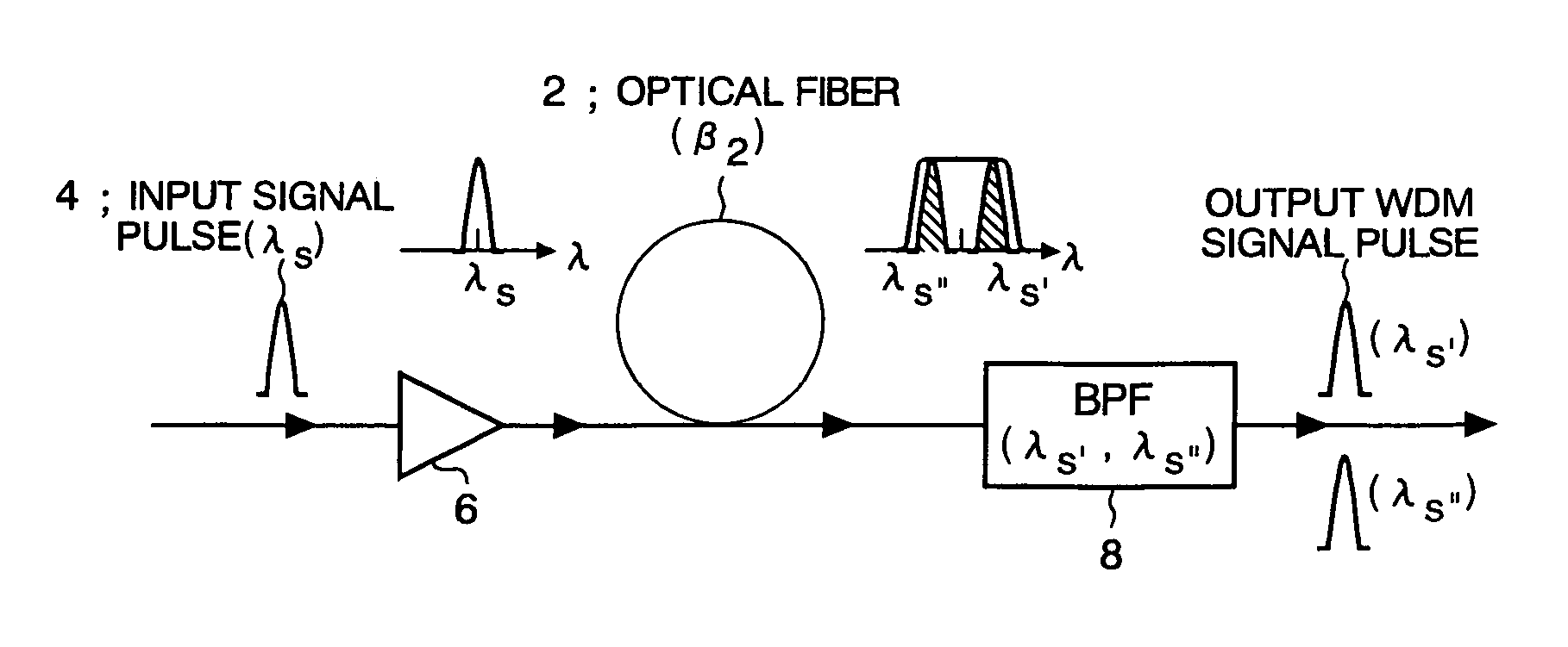
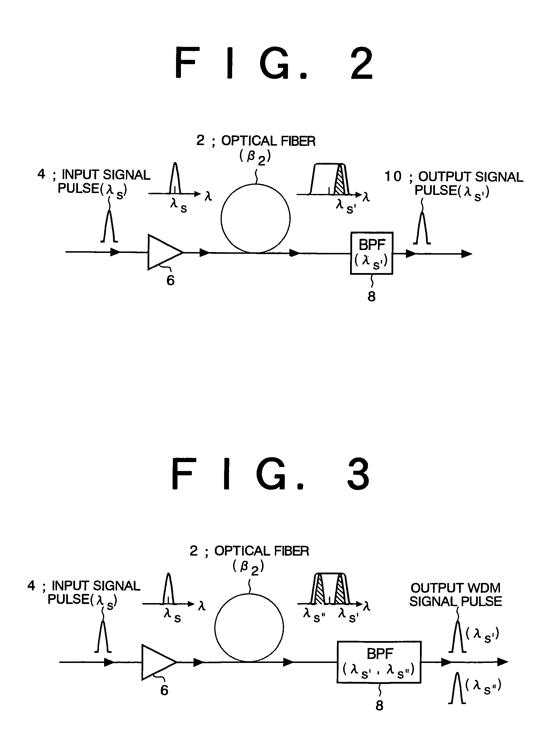
[0041]Some preferred embodiments of the present invention will now be described in detail with reference to the attached drawings.

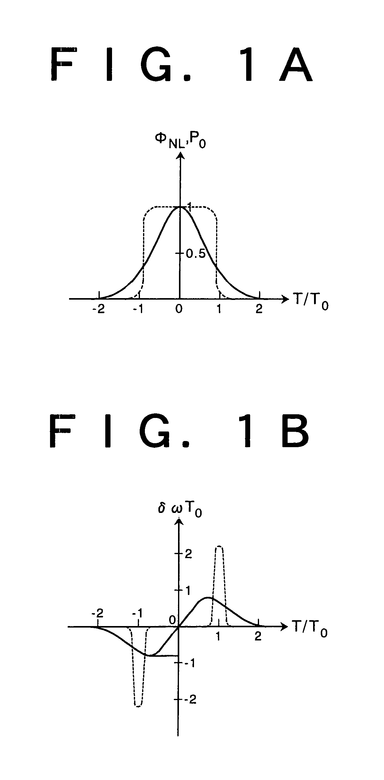
[0042]Now consider the case that an optical pulse U(z,T) having a width T0 and a peak power P0 propagates in an optical fiber, where T is time in a coordinate system moving with the optical pulse. In the case that the chromatic dispersion β2 of this optical fiber is not so large and the dispersion length LD=T02 / |β2| is sufficiently larger than the nonlinear length LNL=1 / γP0 (γ is the third-order nonlinear coefficient) to the optical pulse (LD>>LNL), the phase shift øNL(z,T) by SPM (self-phase modulation) is expressed as follows:

[0043]ϕNL⁡(z,T)=U⁡(0,T)2⁢ZeffLNL(1)

where zeff=[1−exp(−αz)] / α is the effective (nonlinear) interaction length.

[0044]In this case, the chirp δωNL is given by the following expression.

[0045]δωNL=∂ϕNL∂T=-∂U⁡(0,T)2∂T⁢zeffLNL(2)

where |U(0,T)|2 corresponds to the peak power, so that Eq. (2) shows that the chirp of the optical pulse become...


PUM

PropertyMeasurementUnit
lengthaaaaaaaaaa
lengthaaaaaaaaaa
wavelengthaaaaaaaaaa

Abstract

The present invention relates to a method for processing an optical signal is provided. An optical signal is input into an optical waveguide structure for providing a nonlinear effect. As a result, the optical signal undergoes chirping induced by the nonlinear effect. An output optical signal output from the optical waveguide structure is supplied to an optical bandpass filter to thereby extract components except a small-chirp component from the output optical signal. The optical bandpass filter has a pass band including a wavelength different from the wavelength of the optical signal. By extracting the components except the small-chirp component from the output optical signal in the form of pulse, it is possible to remove intensity fluctuations or accumulated noise especially at a top portion and / or a low-power portion of the pulse.

Description

CROSS-REFERENCE TO RELATED APPLICATION[0001]This application relates to application Ser. Nos. 09 / 560,723, 09 / 571,384, 09 / 637,640, and 09 / 665,164, and which are incorporated herein by references.BACKGROUND OF THE INVENTION[0002]1. Field of the Invention[0003]The present invention relates to a method, device, and system for processing an optical signal.[0004]2. Description of the Related Art[0005]In an optical fiber communication system that has been put to practical use in recent years, a reduction in signal power due to transmission line loss, coupling loss, etc. is compensated by using an optical amplifier such as an erbium doped fiber amplifier (EDFA). The optical amplifier is an analog amplifier, which functions to linearly amplify a signal. In this kind of optical amplifier, amplified spontaneous emission (ASE) noise generated in association with the amplification is added to cause a reduction in signal-to-noise ratio (S / N ratio), so that the number of repeaters is limited to re...

Claims


Application Information

Patent Timeline
Patent Type & Authority Patents(United States)
IPC IPC(8): H04B10/00G02F1/365H04B10/2507H04B10/2519H04B10/2525H04B10/299H04J14/00H04J14/02
CPCH04B10/299H04B2210/258
Inventor WATANABE, SHIGEKIFUTAMI, FUMIO
Owner FUJITSU LTD
Why Eureka
Try Eureka