Wavelength conversion device with avalanche multiplier

a conversion device and wavelength technology, applied in the field of photonics, can solve the problems of complicated manufacturing and high cost of arrays, and achieve the effect of improving device performan

Inactive Publication Date: 2006-07-18
NAT RES COUNCIL OF CANADA
View PDF8 Cites 21 Cited by
  • Summary
  • Abstract
  • Description
  • Claims
  • Application Information

AI Technical Summary

Benefits of technology

[0013]The resulting integrated device will detect an incoming infrared (IR) signal, amplify the signal photocurrent, and then convert the amplified signal back to IR light with a shorter wavelength. With the amplification of the incorporated avalanche multiplier, the incoming infrared image will be significantly intensified and converted to the outgoing image. Current from the photodetector (PD) resulting from the impingement of IR radiation typically in the wavelength range of 1.1 to 1.65 μm is amplified by the avalanche multiplier, and drives the LED to emit photons with shorter wavelength, e.g., at 872 nm or visible light range. The output energy can be efficiently detected by a silicon CCD (charge coupled device). The integrated device can thus act as a solid-state image intensifier in addition to a wavelength up-converter.
[0014]Wavelength up-conversion from a range of 1.1–1.65 μm to below 1.0 μm (e.g., 872 nm or 923 nm) permits the highly-efficient detection by a silicon-based CCD camera. In a preferred embodiment, wafer fusion technology permits the exploitation of the best performance of each functioning unit in a single device by optimizing the epitaxial layers independently.
[0015]Methods for making pixelized and pixelless QWIP-LED imaging devices are described in the afore-mentioned U.S. Pat. No. 5,567,955 and U.S. Pat. No. 6,028,323, respectively. These methods can be used for making pixelized and pixelless imaging devices using the wavelength converter of the invention. The device micro-fabrication mainly involves mesa etching for device isolation and metal depositions for electrical contacts. Additional steps such as depositions of anti-reflection coatings and fabrication of micro-lens on device top surface may be taken for improving device performance.
[0022]In accordance with yet another embodiment, further measures, including the fabrication of micro-lens on device emission surface and the deployment of a micro-cavity enhancement effect, can be taken to improve the device performance.

Problems solved by technology

Such arrays are complicated to manufacture and costly.

Method used


Image

  • Wavelength conversion device with avalanche multiplier
  • Wavelength conversion device with avalanche multiplier
  • Wavelength conversion device with avalanche multiplier

Examples


Embodiment Construction

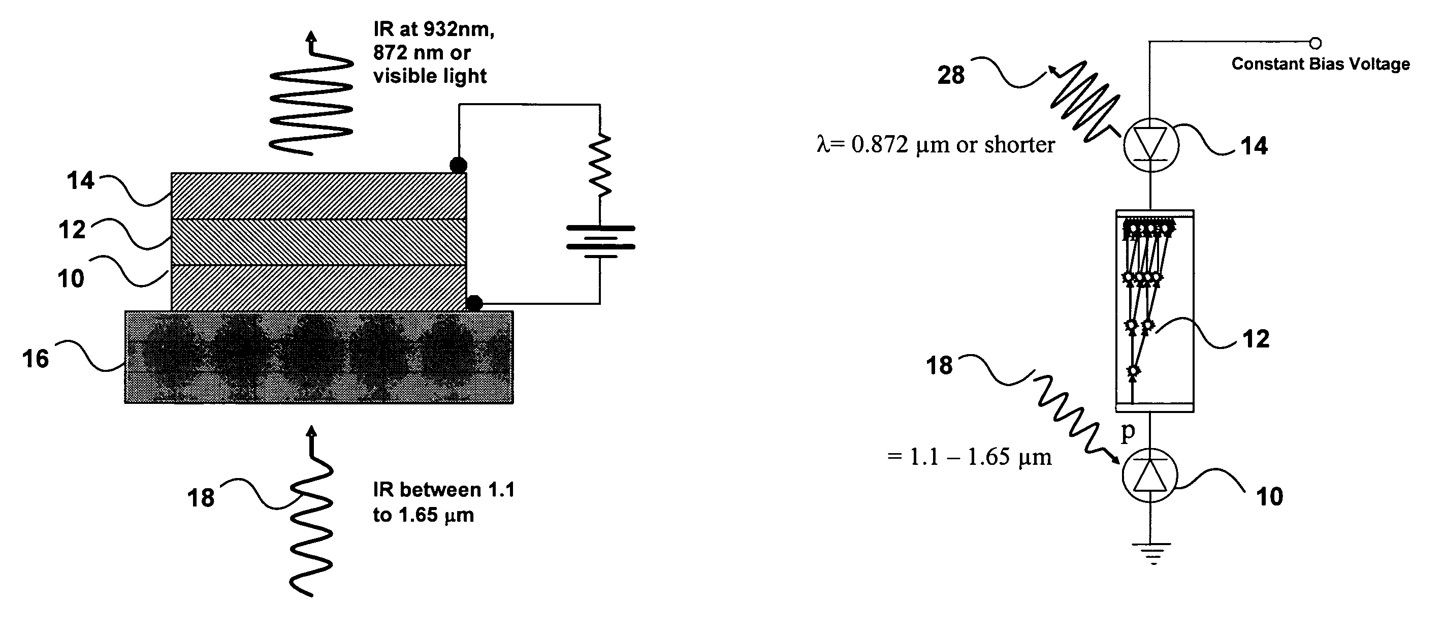
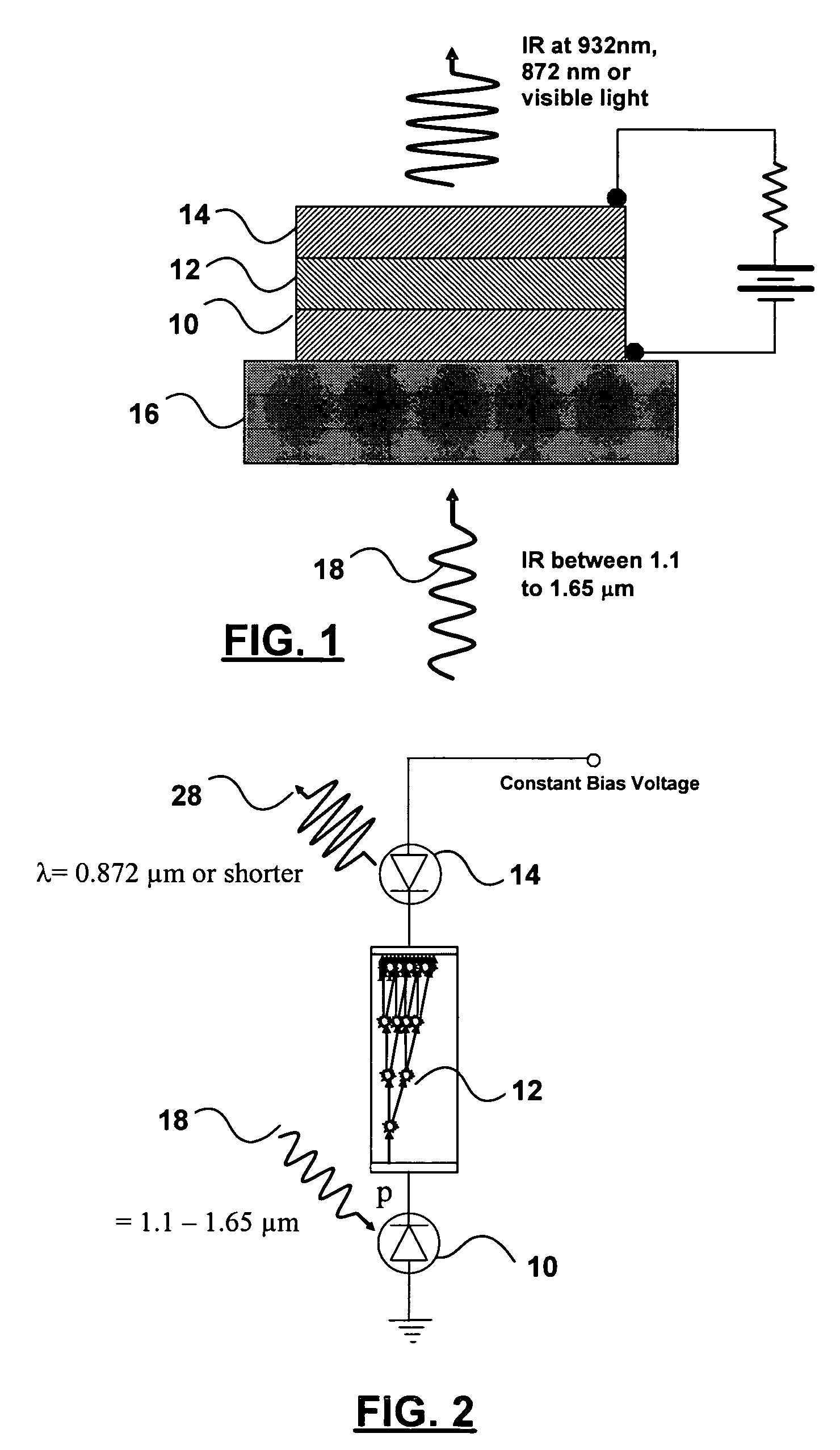
[0039]FIG. 1 illustrates in schematic form one embodiment of the invention in its most basic form.

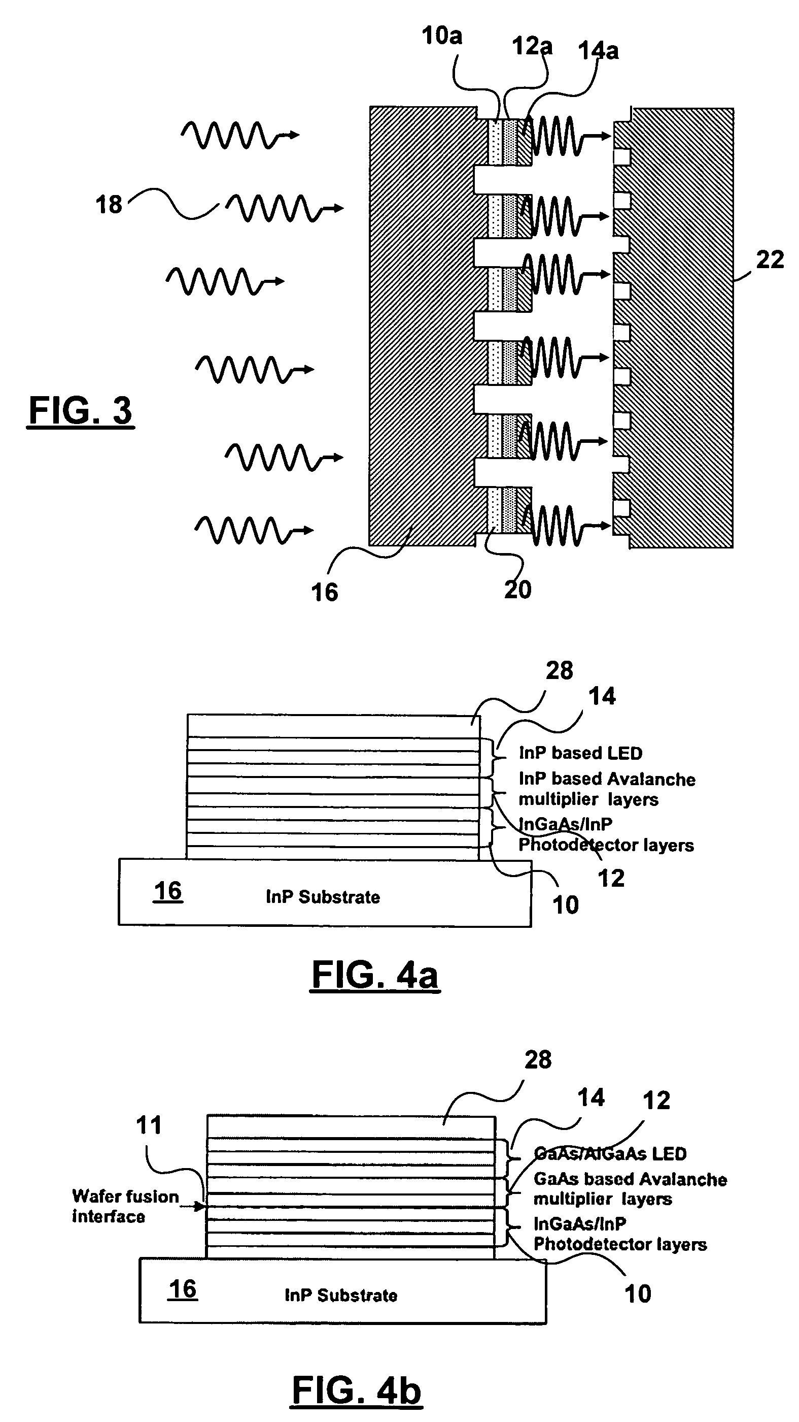
[0040]A photodetector (PD) 10, an avalanche multiplier 12, and an LED 14 are integrated on a substrate 16 in a stacked arrangement. The substrate 16 is transparent to the incoming IR energy (in wavelength range of 1.1 to 1.65 μm) to pass through it to the photodetector 10.

[0041]Upon application of a bias current, e.g. from a battery via a load resistor, to the stacked PD 10, avalanche multiplier 12 and LED 14 in series, the same current passes through all of the components. The incoming IR energy 18 generates signal photocurrent in the PD component 10, which is substantially amplified by the avalanche multiplier 12 and passes into the LED 14.

[0042]The increase of bias current due to the generation and amplification of the signal photocurrent leads to the increase of LED emission at 0.87 μm (or 0.932 μm, or visible light wavelength, depending on the materials used for the LED active regi...


PUM

PropertyMeasurementUnit
wavelengthaaaaaaaaaa
peak wavelengthaaaaaaaaaa

Abstract

A wavelength conversion device includes a photodetector for generating a photocurrent in response to the detection of radiation at a first wavelength. An avalanche multiplier amplifies the signal photocurrent and feeds this to a light emitting element that produces radiation at a second wavelength shorter than the first wavelength and corresponding to the detected radiation at the first wavelength. The components are assembled together in an integrated stacked arrangement either by epitaxial growth or wafer fusion of the individual components. The device is useful as an image intensifier or thermal imaging device.

Description

FIELD OF THE INVENTION[0001]This invention relates to the field of photonics, and in particular to a wavelength conversion device for converting radiation from one wavelength to another, and a method of making such a device.BACKGROUND OF THE INVENTION[0002]Infrared imaging is widely used in a variety of applications including night vision, surveillance, search and rescue, remote sensing, and preventive maintenance. Imaging devices for these applications, which must be able to detect near, mid and far infrared light, are typically constructed from InGaAs, InSb and HgCdTe focal plane arrays. Such arrays are complicated to manufacture and costly.[0003]Alternatively, quantum well infrared photodetectors (QWIPs) can detect mid and far infrared light. QWIP devices are described in U.S. Pat. No. 4,873,555, issued Oct. 10, 1989 to the University of Pittsburgh and in U.S. Pat. No. 4,894,526 issued Jan. 16, 1990 to American Telephone and Telegraph Company, AT&T Bell Laboratories. The latter p...

Claims


Application Information

Patent Timeline
Patent Type & Authority Patents(United States)
IPC IPC(8): G02F2/02H01S5/50G02B23/12H01L27/15H01L31/14H01L31/18H01L33/08H04N5/33
CPCH01L27/15H01L31/0232H01L31/173H01L31/0352H01L33/08H01L31/02327
Inventor CHUN LIU, HUIBAN, DAYANLUO, HUI
Owner NAT RES COUNCIL OF CANADA
Why Eureka
Try Eureka