High-aspect-ratio-microstructure (HARM)

a technology of high-aspect ratio and microstructure, applied in the direction of fluid pressure measurement, generator/motor, instruments, etc., can solve the problems of large system size and volume, heavy and complicated manufacturing method of high-aspect ratio microstructure (harm) having a height difference, and achieve the effect of significantly simplifying the manufacturing process of harm

Inactive Publication Date: 2006-08-08
WALSIN LIHWA
View PDF14 Cites 12 Cited by
  • Summary
  • Abstract
  • Description
  • Claims
  • Application Information

AI Technical Summary

Benefits of technology

[0012]It is one object of the present invention to provide a selective etching method with lateral protection function, which employs a boron ion diffusion process. The boron-doped silicon with the feature of stopping the etching is applied to the structure so as to form a lateral strengthening structure. Since the lateral strengthening structure provides protection for the peripheral wall, the selective etching can be achieved that partial structure is released through silicon wet-etching. On the other hand, the lateral strengthening structure formed through the boron diffusion mechanism not only has the feature of being insulating to the silicon substrate, but also provides the electricity-conductive function.
[0013]It is another object of the present invention to provide a selective etching method for manufacturing a high-aspect-ratio-microstructure (HARM) that not only the upper structure and the lower structure are formed simultaneously, but also only three photo masks are needed in the manufacturing process. The upper structure and the lower structure of the generated HARM have a height difference therebetween, which renders the upper surface of the generated HARM an uneven surface. Hence, the manufacturing process for the HARM is significantly simplified.
[0014]It is another object of the present invention to provide a manufacturing process for a high-aspect-ratio-microstructure (HARM) that the interval distance between the upper and lower structures of the generated HARM is maintained short. Further, the thickness of any portion of the generated HARM can be adjusted in the manufacturing process according to different needs.

Problems solved by technology

With the advance of the modern technology, the system size and volume have been smaller and more delicate.
However, the manufacturing method for a high-aspect-ratio-microstructure (HARM) having a height difference is still heavy and complicated.
From the above description, it is known that the manufacturing method for the HARM having a height difference is still very complex.
When a manufacturing process has too many steps, the quality and the stability of each step are hard to control, which might result in an unstable manufacturing process.
Therefore, the allowable alignment error is quite small.
In addition, the above manufacturing process for the silicon chip often has the unavoidable problem of not having enough conductive depth for the structure.
Since the doped depth of silicon is mostly limited within 10 micrometer, the deeper part of the thick structure is usually not conductive, which affects the actuation and the detection feature.
However, this solution still generates other problems in the latter manufacturing process, such as the difficulty for chip connection, the hardship to attach a metal lateral wall on the structure, and the machining limitation.
However, the accomplished structure obtained from the above manufacturing process can only have one identical thickness.
The thickness of the body structure can not be maintained if the thickness of the distortion axis is trimmed or decreased.
Therefore, the conventional manufacturing process has a certain limitation for the thickness of the elastic spring (deformation).

Method used


Image

  • High-aspect-ratio-microstructure (HARM)
  • High-aspect-ratio-microstructure (HARM)
  • High-aspect-ratio-microstructure (HARM)

Examples


Embodiment Construction

[0061]The present invention will now be described more specifically with reference to the following embodiments. It is to be noted that the following descriptions of preferred embodiments of this invention are presented herein for purpose of illustration and description only; it is not intended to be exhaustive or to be limited to the precise form disclosed.

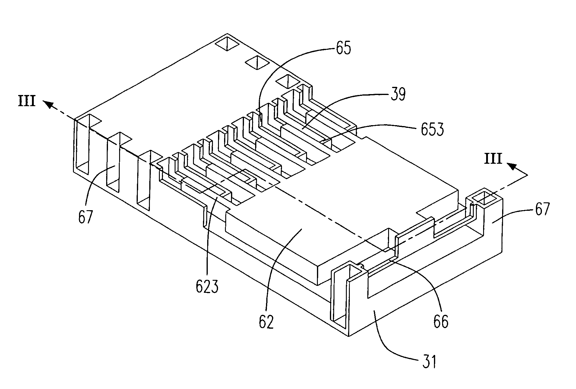
[0062]Please refer to FIGS. 3(a)–(f). FIGS. 3(a)–(f) are diagrams illustrating the steps of the manufacturing method for a high-aspect-ratio-microstructure (HARM) according to a preferred embodiment of the present invention. FIGS. 3(a)–(f) show the sectional view of the HARM. Firstly, a silicon substrate 31 is provided. The first mask layer 32 having plural openings 35 is formed on the silicon substrate 31. The second mask layer 33 is formed on the first mask layer 32. As shown in FIG. 3(a), the second mask layer 33 is then formed in at least one of openings 35 for covering at least one part of the silicon substrate 31. Next, as ...


PUM


Abstract

A high-aspect-ratio-microstructure (HARM) is provided. The structure includes: a substrate; a lower structure with a comb shape fixedly mounted on said substrate and having first plural comb fingers, wherein each of the first plural comb fingers has a thin slot thereon; an upper structure with a comb shape having second plural comb fingers, wherein the lower structure and the upper structure have a height difference therebetween so as to form an uneven surface; and a lateral strengthening structure formed at vertically peripheral walls of the first plural comb fingers and the second plural comb fingers for protecting the plural first and second comb fingers.

Description

FIELD OF THE INVENTION[0001]The present invention is related to a structure applied in the Micro-Electro-Mechanical System (MEMS), and more particularly, to a high-aspect-ratio-microstructure (HARM) which is applied to an actuator.BACKGROUND OF THE INVENTION[0002]Nowadays, the Micro-Electro-Mechanical System (MEMS) is a newly developed field that every country in the world is actively interfering and participating in. MEMS is a miniature system which generates a predict movement. With the advance of the modern technology, the system size and volume have been smaller and more delicate. The system miniaturization has led to many advantages. (1) Mass production: Several hundreds to several thousands of mechanical components can be formed on a single one silicon chip at the same time. Similar to the IC manufacture, the manufacture cost can be reduced accordingly. (2) Miniaturization: A quite small but still having high accuracy mechanical component can be produced by applying the method...

Claims


Application Information

Patent Timeline
Patent Type & Authority Patents(United States)
IPC IPC(8): H02N1/00G02B26/08B81B3/00
CPCH02N1/008B81C1/00595B81B2201/033Y10S438/942
Inventor HSIEH, JERWEICHU, HUAI-YUANTSAI, JULIUS MING-LINFANG, WEILEUN
Owner WALSIN LIHWA
Why Eureka
Try Eureka