Method and apparatus for reducing soft error rate in SRAM arrays using elevated SRAM voltage during periods of low activity

a technology of sram array and sram voltage, which is applied in the field of reducing soft error rate in sram memory, can solve the problems of large amount, large alpha particles, and large high value resistors in semiconductor structures, and achieve the effect of reducing a soft error ra

Active Publication Date: 2006-08-15
MONTEREY RES LLC
View PDF5 Cites 9 Cited by
  • Summary
  • Abstract
  • Description
  • Claims
  • Application Information

AI Technical Summary

Benefits of technology

[0014]The current invention teaches methods and apparatus that provide for reducing...

Problems solved by technology

Lead is subject to radioactive decay, resulting in alpha particles.
Unfortunately, high value resistors in semiconductor structures tend to be relatively large.
Also, they typically have a relatively large amount of parasitic capacitance that slows the process of writing data into the SRAM memory cell.
Slower regeneration also degrades performance when writing operations to the SRAM memory cell.
However, adding capacitors causes a less dense SRAM memory cell, as well as poorer performance.
SOI (Silicon On Insulator) semiconductor t...

Method used


Image

  • Method and apparatus for reducing soft error rate in SRAM arrays using elevated SRAM voltage during periods of low activity
  • Method and apparatus for reducing soft error rate in SRAM arrays using elevated SRAM voltage during periods of low activity
  • Method and apparatus for reducing soft error rate in SRAM arrays using elevated SRAM voltage during periods of low activity

Examples


first embodiment

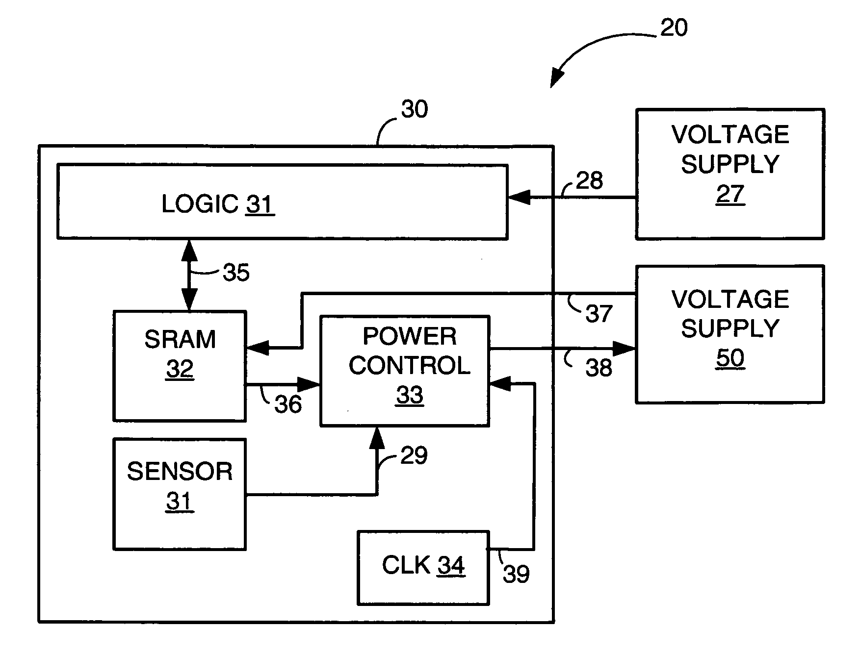
[0048]power control 33 is shown in FIG. 4A. This embodiment causes Vdd to be increased from the first voltage value to the second (higher) voltage value if a particular number of cycles of clock 34 have occurred without the SRAM 32 reporting an access on signal 36. The particular number of clock cycles (at a particular frequency) represents a time interval specified by the designer of electronic system 20. A compare value 40 is loaded during startup of electronic system 20, or, alternatively, is simply hardwired into compare value 40. For example, in a computer system embodiment of electronic system 20, a value is scanned or otherwise written into compare value 40. The value for the particular number of cycles is written into compare value 40 is chosen by the designer to satisfy the time interval according to the designer's requirements regarding power dissipated, and, perhaps, the designer's knowledge of applications that are run on electronic system 20. A large value will cause Vd...

second embodiment

[0049]power control 33 is shown in FIG. 4B. In this embodiment, if an SRAM 32 is used at more than a predetermined access rate, the Vdd is set to a first voltage value; if the SRAM 32 is used less than the predetermined access rate, Vdd is set at a second voltage value. The first voltage value is less than the second voltage value.

[0050]Power control 33 in the embodiment of FIG. 4B has a compare value 49, that, like compare value 40 of FIG. 4B, is hardwired or written by other portions (not shown) of an electronic system based on a designer's choice of tradeoff between power dissipated in electronic system 20 and SER. Compare value 49 contains an access rate limit specified by the designer. A counter 46 counts up responsive to the clock signal on signal 39, output by clock 34. Counter 46 counts down responsive to a signal on signal 36, scaled by scale 47. For example, if the SRAM 32 can be accessed, at most, four times for each cycle of clock 34, in an exemplary embodiment, scale 47...

third embodiment

[0053]FIG. 4C shows power control 33. This embodiment provides for two or more values of Vdd that are selected based on a designer specified relationship between an SRAM access rate and the value of Vdd supplied to the SRAM. Scale 67, signal 68, counter 66 are similar to scale 47, signal 48, and counter 46 as described in reference to FIG. 4B. That is, counter 66 counts up responsive to clock signals from clock 34 (see FIG. 3) sent on signal 39. Counter 66 counts down responsive to SRAM accesses, as scaled by scale 67. At any point in time, therefore, the value of counter 66 contains a value of the SRAM access rate. VID information 69 is hardwired, or is written to from another part of electronic system 20, such as logic 31 (see FIG. 3), with information as to what Vdd should be versus SRAM access rate. Many modern voltage supplies receive a VID (voltage identification) from a semiconductor chip and provide a voltage that is controlled by the value transmitted on the VID. The VID is...


PUM


Abstract

A voltage supplied to an SRAM (static random access memory) in an electronic system is controlled responsive a level of activity in the electronic system. If the level of activity is higher, the voltage is kept lower; if the level of activity, the voltage is increased, reducing soft error rate in the SRAM. For example, one indicator of the level of activity is how frequently the SRAM is accessed. If the SRAM is accessed less frequently, a higher voltage value is used to supply the SRAM than if the SRAM is accessed more frequently. A higher voltage provides a lower soft error rate (SER), but increases power dissipation. The SRAM dissipates less switching power when it is infrequently used and therefore a higher voltage value can be supplied to the SRAM during such times of infrequent use without causing excessive power dissipation by the electronic system.

Description

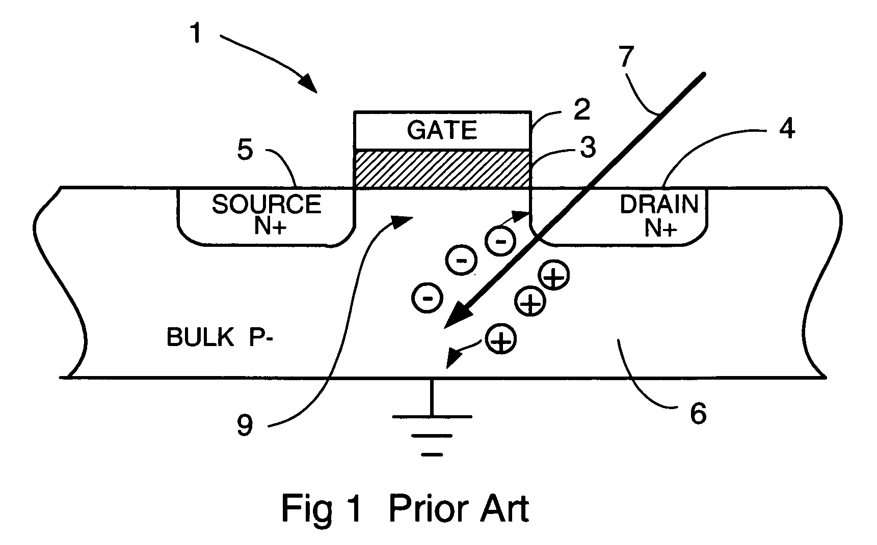
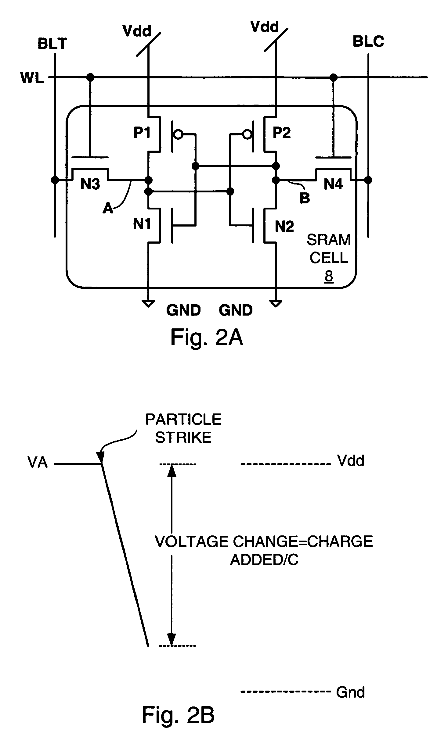
BACKGROUND OF THE INVENTION[0001]1. Field of the Invention[0002]The current invention generally relates to soft error rates in static random access (SRAM) memories. More in particular, the current invention relates to reducing soft error rate in SRAM memories.[0003]2. Description of the Related Art[0004]Electronic systems, and in particular computer systems, typically store a relatively large amount of information in static random access (SRAM) memories on one or more semiconductor chips. For example, a modern computer system might have a 128 KB (128 Kilobytes) of SRAM in a level-1 instruction cache, 128 KB in a level-1 data cache, and 2 MB (Megabytes) in a level-2 cache on a processor chip. Some electronic systems such as computer systems have one or more SRAM chips separate from a logic chip where the logic chip accesses data in the SRAM chips.[0005]SRAM memory cells, i.e., the semiconductor devices on a semiconductor chip that store the “1”s and “0”s used in an SRAM are typically...

Claims


Application Information

Patent Timeline
IPC IPC(8): G11C11/00
CPCG11C11/4125
Inventor AIPPERSPACH, ANTHONY GUSALLEN, DAVID HOWARD
Owner MONTEREY RES LLC
Why Eureka
Try Eureka