Eureka AIR delivers breakthrough ideas for toughest innovation challenges, trusted by R&D personnel around the world.

Light detecting device and method for mounting the same

a technology for detecting devices and light receiving elements, applied in radiation controlled devices, optical radiation measurement, instruments, etc., can solve the problems that the surface mounting technique cannot be applied to the detecting device, and the surface mounting technique cannot be applied to the light receiving element, so as to prevent the incidence, the effect of effective surface mounting, and precise light detection

Active Publication Date: 2006-08-22
FUJIFILM BUSINESS INNOVATION CORP
View PDF8 Cites 13 Cited by
  • Summary
  • Abstract
  • Description
  • Claims
  • Application Information

AI Technical Summary

Benefits of technology

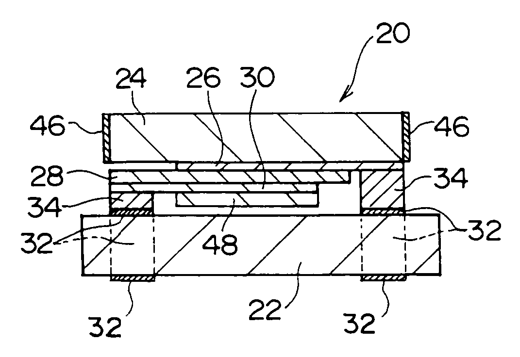
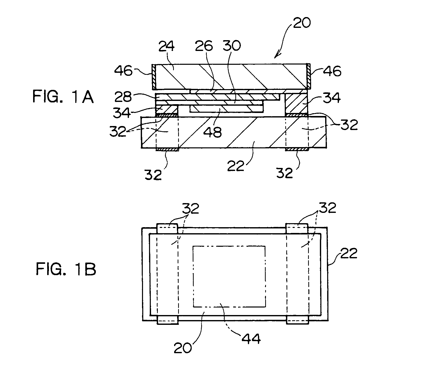
[0012]In the light detecting device of the invention, the light receiving element is arranged on the first face of the insulating substrate and further the second electrode exposed to the first face (for example, the front surface) of the insulating substrate is connected electrically to the semiconductor layer of the light receiving element through the first electrode. When the light detecting device is mounted on, for example, a circuit board, the second electrode exposed to the second face (for example, an end face (side face) or the rear surface) of the insulating substrate is connected electrically to an external terminal of the circuit board. Furthermore, the protective layer may be formed between the light receiving element and the insulating substrate. Therefore, when the light detecting device is worked or mounted, the mechanical strength and the chemical stability (against, for example, heat treatment at the time of the mounting) of the light receiving element can be maintained. For this reason, the light detecting device, which has a simple structure, can be stably surface-mounted on the circuit board or the like without changing the structure of the light receiving element to a large degree.
[0014]In the light detecting device of the invention, it is preferable that the second electrode is a metallic electrode. In this way, the second electrode is made up to the metallic electrode, whereby solder can be used when the light detecting device is electrically connected to, for example, the external terminal of a circuit board. Consequently, more effective surface mounting can be attained.
[0015]In the light detecting device of the invention, it is preferable that the insulating substrate absorbs visible light. The absorption of visible light by the insulating substrate makes it possible to prevent the matter that the light transmitted through the semiconductor layer of the light receiving element is reflected on the insulating substrate so as to be again radiated onto the semiconductor layer. As a result, precise light detection can be attained.
[0016]In the light detecting device of the invention, an example of the structure of the light receiving element is a structure in which the semiconductor layer and the first electrode are formed on a transparent substrate. Moreover, by forming a light-shielding layer on an end face (side face) of the transparent substrate, it is possible to prevent the incidence of light from the end face of the transparent substrate into the light detecting device and improve the light incidence angle characteristic of the device.
[0019]In the light detecting device of the invention, it is preferable that a visible light absorbing layer is formed between the light receiving element and the insulating substrate. The formation of this visible light absorbing layer makes it possible to prevent the matter that the light transmitted through the semiconductor layer of the light receiving element is reflected on the insulating substrate so as to be again radiated onto the semiconductor layer. As a result, precise light detection can be attained.
[0022]The light receiving element and the insulating substrate may be bonded and fixed to each other by applying an adhesive agent onto the entire surface of the light receiving element (except for electrodes for connecting the light receiving element). However, the adhesive agent, a typical example of which is an epoxy adhesive agent, is unstable against ultraviolet rays in many cases. The above-mentioned JP-A No. 2001-210856 makes a suggestion for preventing a deterioration of an epoxy adhesive agent used to bond a light receiving element and a protective member to each other by absorption of ultraviolet rays by a semiconductor layer. However, the absorption by the semiconductor layer is incomplete and this layer transmits the ultraviolet rays. Therefore, a problem about endurance of the adhesive agent remains. Thus, in the invention, the first electrode of the light receiving element and the second electrode of the insulating substrate are electrically connected and bonded to each other through the electrically conductive member at the position different from the light receiving portion of the light receiving element, whereby the light receiving element is bonded and fixed to the insulating substrate and ultraviolet rays transmitted from the light receiving portion which the semiconductor layer constitutes are not radiated onto the bonding portion (the electrically conductive member). As a result, deterioration thereof by the ultraviolet rays can be prevented.

Problems solved by technology

Thus, under the present situation, surface mounting technique cannot be applied to these light receiving elements.
Thus, surface mounting technique cannot be applied to the detecting device.

Method used


Image

  • Light detecting device and method for mounting the same
  • Light detecting device and method for mounting the same
  • Light detecting device and method for mounting the same

Examples


example 1

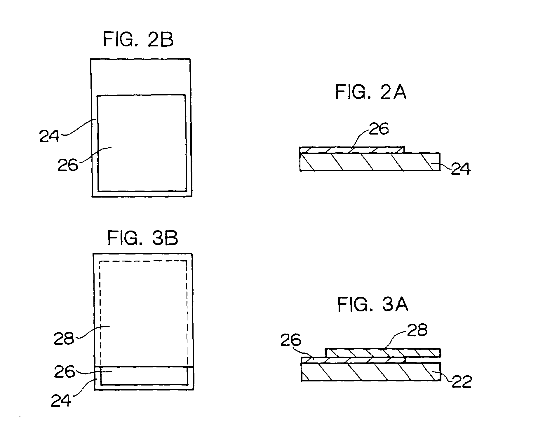
[0090]A substrate in which a metal mask is used to sputter indium tin oxide (ITO) into a thickness of 1000 Å onto a cleaned 0.5 mm thickness borosilicate glass substrate (1.2×1.8 mm) [a transparent substrate 24 in which a transparent conductive electrode 26 is formed] is first put onto the substrate holder 3 set inside the vacuum container, and then the substrate is heated to 400° C. with the heater 4 after the container 1 is evacuated through the air outlet 2. N2 gas introduced at 2000 sccm through the gas introducing pipe 9 into the quartz pipe 5 having a diameter of 25 mm and 2.45 GHz microwaves set into an output of 250 W are supplied through the microwave guide 8 so as to be tuned for matching with a tuner. In this way, electric discharge is caused. At this time, the output of reflected waves is 0 W. H2 gas is introduced at 500 sccm through the gas introducing pipe 10 into the quartz pipe 6 having a diameter of 30 mm. The output of 13.56 MHz high-frequency waves is set into 100...

example 2

[0097]A black silicone resin (silicone adhesive KE 1831, manufactured by Shin-Etsu Chemical Co., Ltd.) is applied into a thickness of 10 μm onto a protective layer formed on a light receiving element, and further a thermosetting electrically conductive paste (an electrically conductive member 34) is dropped onto the respective electrodes (electrode portions for connection) of the light receiving element. While the positioning of the light receiving element is performed, the light receiving element is put onto the insulating substrate. The resultant is treated at 160° C. for 30 minutes to connect the terminal electrodes of the insulating substrate electrically to the respective electrodes of the light receiving element through the electrically conductive paste and further bond and fix the light receiving element onto the insulating substrate. Furthermore, a visible light absorbing layer 50 adhered closely to the protective layer is formed. In the same manner as in Example 1 except th...

example 3

[0100]The same silicone resin as in Example 1 is screen-printed on a light receiving element to form a protective layer of 10 μm thickness. Furthermore, the same silicone resin as in Example 2 is screen-printed on an insulating substrate to form a black visible light absorbing layer. In the same way as in Example 2 except that these are used, a light detecting device in which the protective layer is adhered closely to the visible light absorbing layer is produced. The spectral sensitivity of this light detecting device is not different from that of Example 2 in the ultraviolet ray range or the visible light range.

[0101]The terminal electrodes exposed to the end faces of the insulating substrate are mounted on creamy solder printed on an electric circuit board so as to position the produced light detecting device. The resultant is subjected to heat treatment at 250° C. for 30 seconds. As a result, the light detecting device is permitted to be surface-mounted onto the circuit board.

[0...


PUM


Abstract

A light detecting device is fabricated to have the following structure: a light receiving element having a protective layer, in which a transparent conductive electrode, a semiconductor layer, an electrode and the protective layer are successively formed on a transparent substrate, is arranged on a first face of an insulating substrate having a terminal electrode formed to be exposed to first and second faces of the insulating substrate in such a manner that the protective layer is opposed to the first face of the insulating substrate; and further the transparent conductive electrode and the electrode are connected electrically to the terminal electrode exposed to the first face of the insulating substrate. The light detecting device having this structure is surface-mounted on a circuit board to connect the terminal electrode exposed to the second face of the insulating substrate to an external terminal of the circuit board.

Description

CROSS-REFERENCE TO RELATED APPLICATION[0001]This application claims priority under 35USC 119 from Japanese Patent Application No. 2003-104474, the disclosure of which is incorporated by reference herein.BACKGROUND OF THE INVENTION[0002]1. Field of the Invention[0003]The present invention relates to a light detecting device such as an ultraviolet ray detecting device.[0004]2. Description of the Related Art[0005]In recent years, industrial instruments using ultraviolet rays have been spread in many devices such as color image outputting devices, ozone generating devices and semiconductor fabricating devices, and many fields such as printing, painting and optical shaping fields. In order to measure ultraviolet rays, a semiconductor light receiving element is used.[0006]As the semiconductor light receiving element, an element made of a semiconductor which absorbs no visible light, such as an element made of a gallium nitride type semiconductor or an oxide type semiconductor, is suggeste...

Claims


Application Information

Patent Timeline
Patent Type & Authority Patents(United States)
IPC IPC(8): H01L31/0203H01L31/02G01J1/42
CPCG01J1/429G01J1/42
Inventor YAGI, SHIGERUKOJIMA, HIROSHIKURITA, SHIGERU
Owner FUJIFILM BUSINESS INNOVATION CORP
Why Eureka
Eureka Blog
Learn More