Plasma processing apparatus, method for operating the same, designing system of matching circuit, and plasma processing method

a plasma processing and apparatus technology, applied in the direction of plasma technique, coating, electric discharge lamps, etc., can solve the problems of plasma not being discharged, the exact impedance z of the user's plasma processing apparatus cannot be provided, and the plasma cannot be produced. , to achieve the effect of reducing cost, rapid production, and reducing power loss

Active Publication Date: 2006-08-22
ALPS ALPINE CO LTD +1
View PDF7 Cites 51 Cited by
  • Summary
  • Abstract
  • Description
  • Claims
  • Application Information

AI Technical Summary

Benefits of technology

[0055]Since the engineer can obtain the data for the impedance Z1 of the plasma processing chamber even though the chamber is remote from the engineer, the product matching circuit can be rapidly produced at reduced cost.
[0056]In the matching circuit designing system, the plasma processing chamber preferably includes impedance measuring means for measuring the impedance Z0 of the plasma processing chamber before plasma discharge and for outputting the impedance Z0 to the designing means. The engineer can optimize the adjustable range of the matching circuit based on the obtained impedances Z0 and Z1. Thus, the product matching circuit has...

Problems solved by technology

Thus, the actual impedance Z1 of their apparatuses cannot be provided as design information by the apparatus manufacturer and the RF generator manufacturer on a delivery of the apparatuses to users.
Furthermore, a user of the plasma processing apparatus cannot know the exact impedance Z0; hence, the control circuit 14 cannot adjust the output impedance of the matching circuit 2C to the impedance Z0 in some cases.
In such cases, plasma is not discharged because of impedance mismatching.
Furthermore, the impedance Z1 of the matching circuit 2C after plasma discharge is not stored in the conventional plasma processing apparatus; thus, the adjustment of the output impedance to the impedance Z1 also requires many hours of work.
Thus, the effect of the plasma discharge decreases due to mismatching.
Unfortunately, this results in a large parasitic ...

Method used


Image

  • Plasma processing apparatus, method for operating the same, designing system of matching circuit, and plasma processing method
  • Plasma processing apparatus, method for operating the same, designing system of matching circuit, and plasma processing method
  • Plasma processing apparatus, method for operating the same, designing system of matching circuit, and plasma processing method

Examples


first embodiment

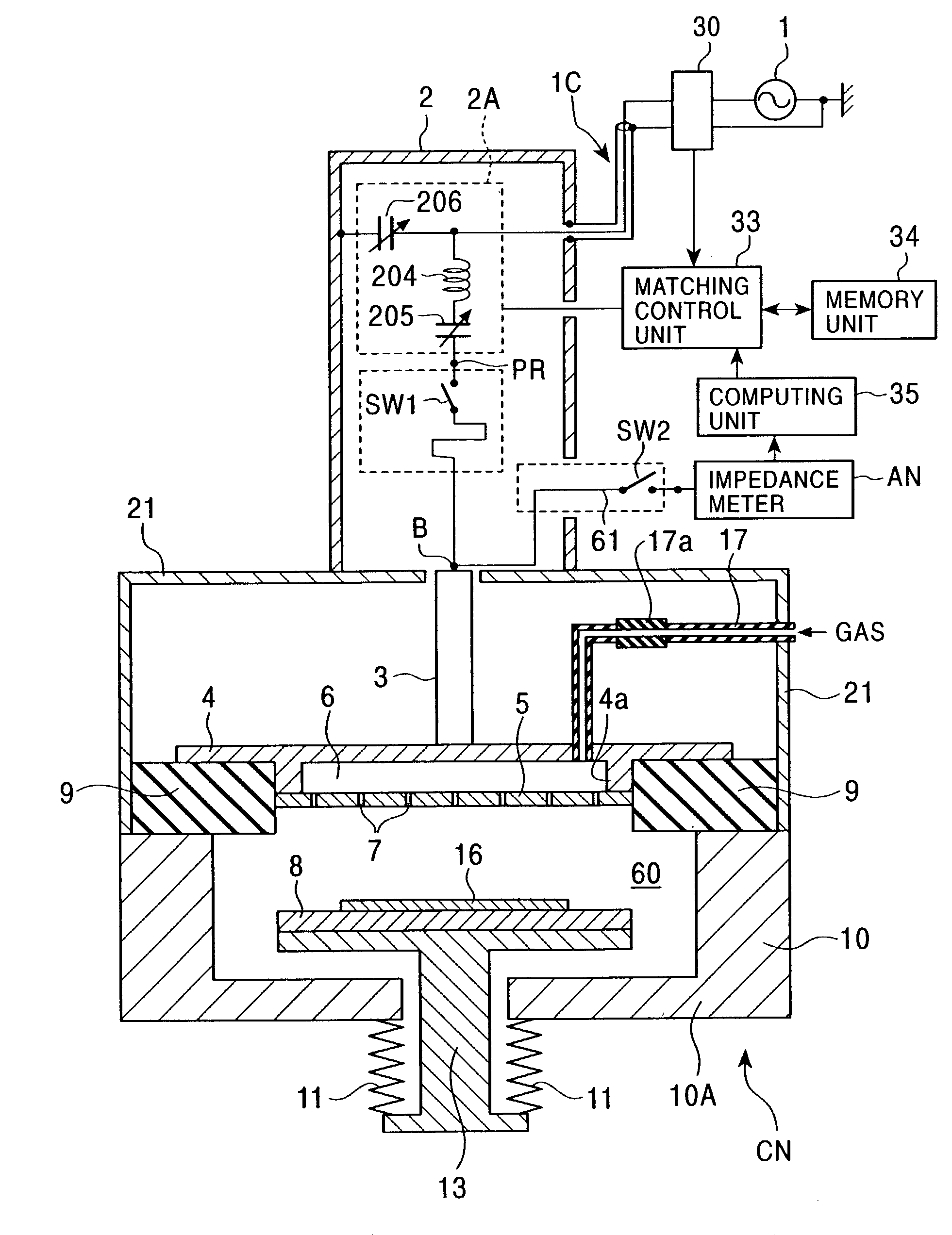
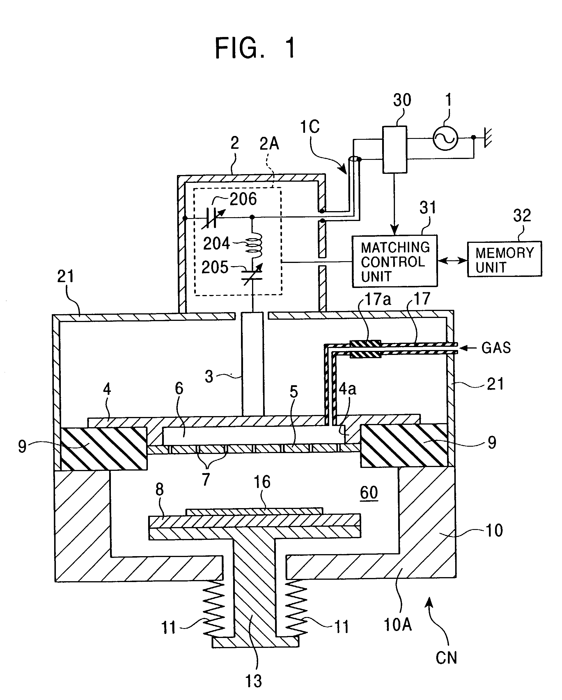
[0075]FIG. 1 is a schematic view of a plasma processing apparatus according to a first embodiment of the present invention. Parts having the same functions as in FIG. 15 are referred to with the same reference numerals, and a detailed description thereof with reference to drawings has been omitted.

[0076]The plasma processing apparatus of the first embodiment is of a single-frequency excitation type and is used for plasma treatments, such as chemical vapor deposition (CVD), sputtering, dry etching, and ashing. The plasma processing apparatus includes a plasma processing chamber CN having parallel plate electrodes 4 and 8 (a plasma excitation electrode 4 and a susceptor electrode 8), an RF generator 1 connected to the plasma excitation electrode 4 through a feed plate 3, and a matching circuit 2A that performs the impedance matching between the plasma processing chamber CN and the RF generator 1, the latter value represented by the characteristic impedance of a coaxial cable 1C.

[0077]...

second embodiment

[0123]FIG. 6 is a schematic view of a plasma processing apparatus according to a second embodiment of the present invention. Parts having the same functions as in FIG. 1 are referred to with the same reference numerals, and a detailed description thereof with reference to drawings has been omitted.

[0124]Selected main components in the present invention, i.e., a reflected wave detector 30, a matching control unit 33, a memory unit 34, and a computing unit 35, which are disposed in the vicinity of a matching box 2, will now be described in detail.

[0125]A radio frequency generator 1 supplies RF power for plasma discharge to a plasma processing chamber CN via the reflected wave detector 30 and the matching box 2.

[0126]A matching circuit 2A is disposed in the matching box 2 for matching the output impedance of the radio frequency generator 1 with the load impedance of the plasma processing chamber CN. The matching circuit 2A includes a load capacitor 206, a tuning inductor 204, and a tun...

third embodiment

[0149]FIG. 8 is a schematic diagram of a configuration of a matching apparatus designing system for a plasma processing apparatus according to a third embodiment. In the drawing, the structure of the matching circuit 2A of the matching circuit 2A in the matching box 2 is illustrated.

[0150]In this embodiment, the plasma processing apparatus is placed at an operation site 300. A matching circuit 2A (FIG. 8) or 2B (FIG. 9) is provided between the plasma processing chamber CN and the radio frequency generator 1 of the plasma processing apparatus.

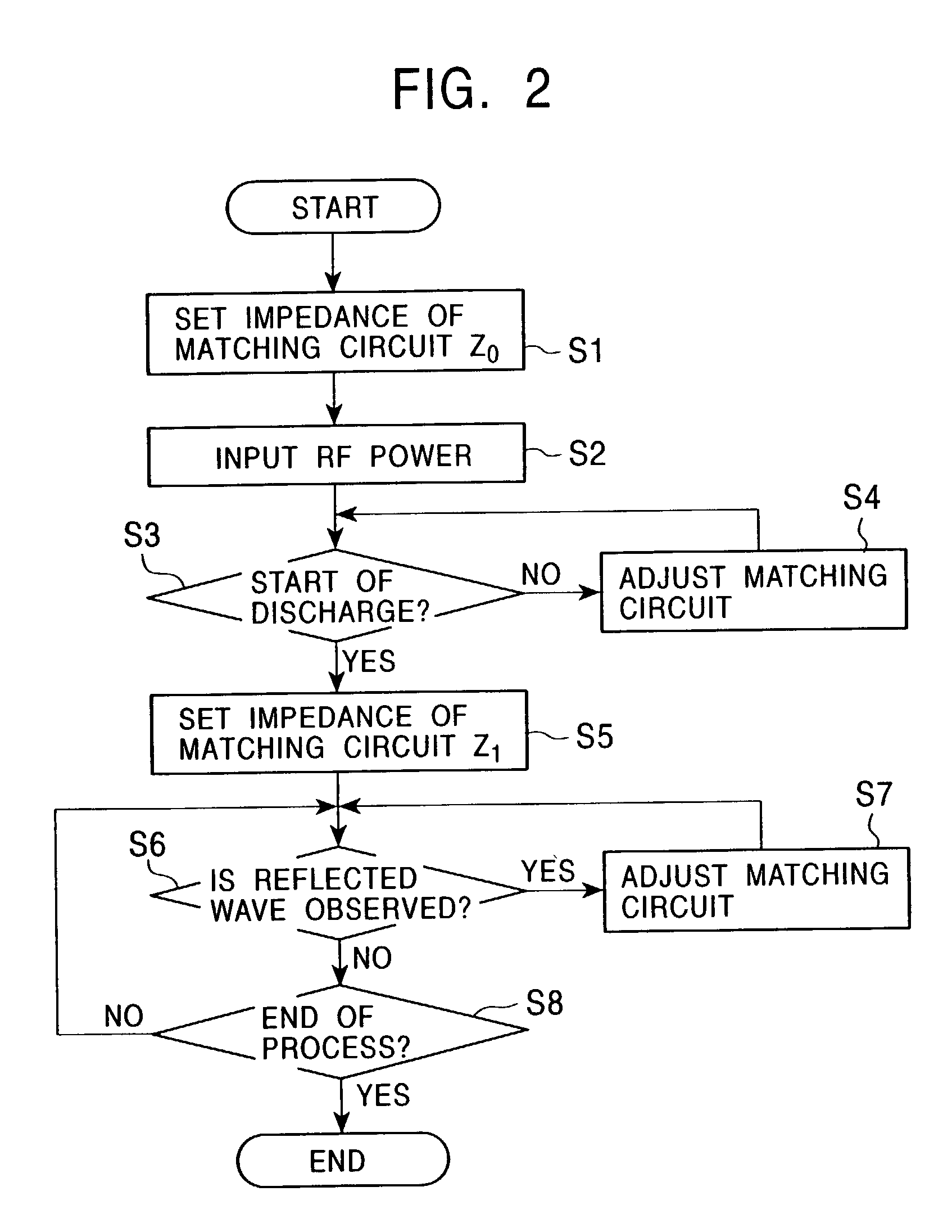
[0151]In the initialization process of the plasma processing apparatus, the matching circuit 2A is used for adjustment. Impedance matching is performed with a drive control unit 51, a reflected wave measuring unit 50, and a displacement-measuring unit 52. The displacement of the matching circuit 2A at the impedance matched state is transmitted from a user terminal 53 to a server 70 at a manufacturer 400 of the matching circuit 2A, for example th...


PUM

PropertyMeasurementUnit
Electric impedanceaaaaaaaaaa

Abstract

A plasma processing apparatus includes a radio frequency generator, a plasma processing chamber, a matching circuit for impedance matching between the radio frequency generator and the plasma processing chamber, and matching circuit adjusting means for matching the output impedance of the matching circuit to the impedance of the plasma processing chamber in a nondischarge state. The matching circuit is a product matching circuit that is produced based on a circuit constant of an adjusting matching circuit. The adjusting matching circuit is disposed between the radio frequency generator and the plasma processing chamber for a required plasma treatment and the circuit constant is determined by impedance matching between the radio frequency generator and the plasma processing chamber so that the adjusting matching circuit matches the load impedance of the plasma processing chamber.

Description

BACKGROUND OF THE INVENTION[0001]1. Field of the Invention[0002]The present invention relates to a plasma processing apparatus used in semiconductor process plasma treatments such as ashing and etching, a method for operating the plasma processing apparatus, and a plasma processing method using the plasma processing apparatus.[0003]The present invention also further relates to a system for designing a matching circuit that matches the load impedance of a plasma processing chamber of the plasma processing apparatus.[0004]2. Description of the Related Art[0005]FIG. 15 shows a typical conventional single-frequency excitation plasma processing apparatus which is used in plasma processes such as a chemical vapor deposition (CVD) process, a sputtering process, a dry etching process, and an ashing process. This plasma processing apparatus includes a matching circuit 2C between a radio frequency generator 1 and a plasma excitation electrode 4. The matching circuit 2C matches the impedance b...

Claims


Application Information

Patent Timeline
IPC IPC(8): H01J7/24C23C16/00H05H1/36H01J37/32
CPCH01J37/32183H01J37/32082H05H1/36
Inventor NAKANO, AKIRAKUMAGAI, TADASHIOBA, TOMOFUMIOHMI
Owner ALPS ALPINE CO LTD
Why Eureka
Try Eureka