Semiconductor device including bit line formed using damascene technique and method of fabricating the same
a damascene and semiconductor technology, applied in the field of semiconductor devices, can solve the problems of complicated photolithographic processes, drams and securing a sufficient process margin, and achieve the effect of easy formation
- Summary
- Abstract
- Description
- Claims
- Application Information
AI Technical Summary
Benefits of technology
Problems solved by technology
Method used
Image
Examples
first embodiment
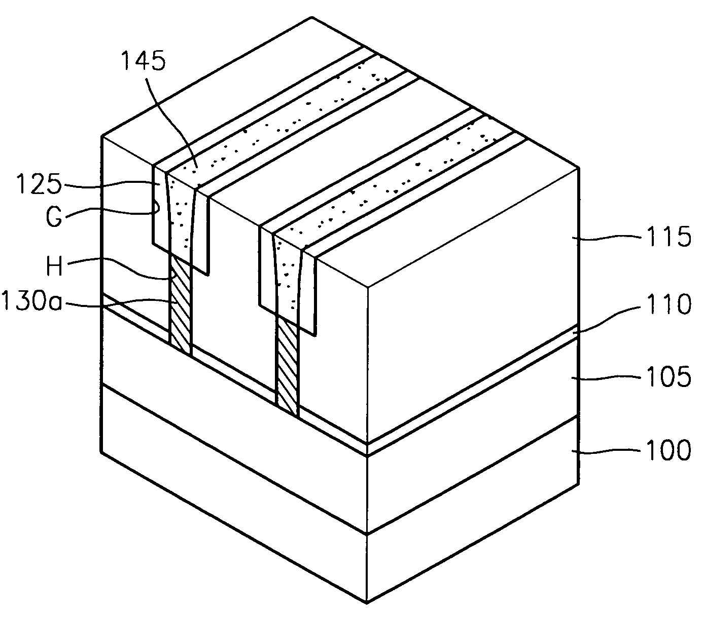
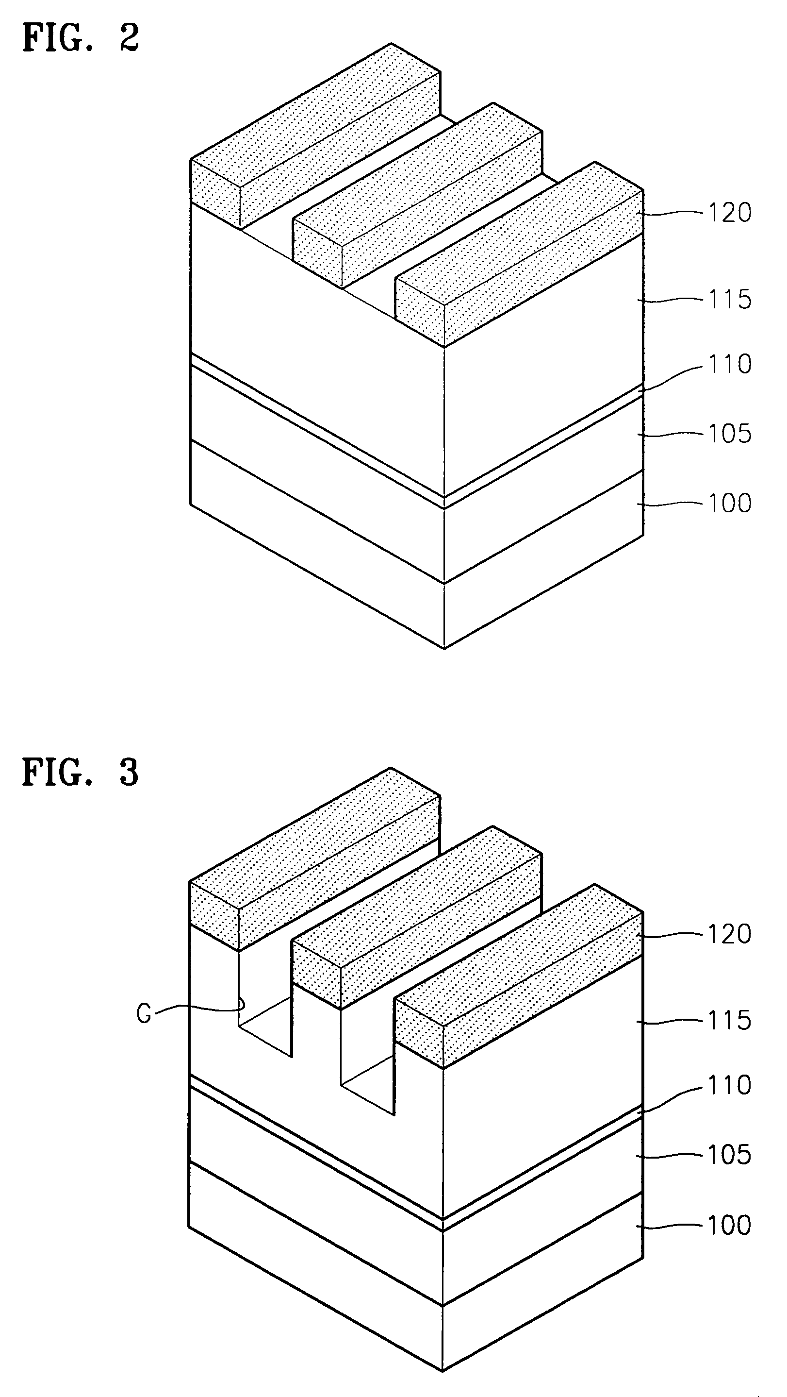
[0022]FIGS. 2 through 9 are cross-sectional views illustrating a method of fabricating a semiconductor device according to the present invention. While the following embodiments will be described with reference to a method of fabricating bit lines of DRAMs, it should be apparent to those skilled in the art that a similar description can be applied to other conductive lines, gate lines, or interconnections.
[0023]Referring to FIG. 2, an etch stop layer 110 and a silicon oxide layer 115 are sequentially formed on a substrate 100 on which a lower structure including an insulating layer 105 is formed. The substrate 100 can be, for example, a single crystalline silicon substrate. The etch stop layer 110 is formed of an insulating material having an etch selectivity with respect to the silicon oxide layer 115. For example, the etch stop layer 110 is formed by depositing a silicon nitride layer to a thin thickness using plasma enhanced-CVD (PE-CVD) or low pressure-CVD (LP-CVD). Also, the et...
second embodiment
[0031]Before the second embodiment is described in detail, characteristics of the present embodiment will be described for clarity. In a DRAM, after a bit line contact plug is formed, a silicon nitride layer, which has an etch selectivity with respect to an interlayer dielectric (ILD) (hereinafter, referred to as a “second insulating layer”), is deposited to a thin thickness. The silicon nitride layer is used as an etch stop layer during the formation of a bit line opening to prevent over-etching of a bit line contact plug of a cell array region. Spacers are formed using, for example, silicon nitride, on the inner walls of the bit line opening. As a result, a bit line can be formed to below the photolithographic limit and the misalignment margin between the bit line and a storage node contact plug can be increased.
[0032]Referring to FIG. 10, a device isolation layer 190 (e.g., a shallow trench isolation (STI) layer) is formed on a substrate 200 to define an active region. While the ...
PUM
 Abstract
Description
Claims
Application Information


