Organic electroluminescent device using optical resonance effect

an electroluminescent device and optical resonance technology, applied in the direction of instruments, discharge tubes, luminescent screens, etc., can solve the problems of low luminance efficiency, disadvantages of conventional organic el devices, low luminance efficiency, etc., and achieve the effect of improving color purity and enhancing luminescen

Active Publication Date: 2006-08-29
SAMSUNG DISPLAY CO LTD
View PDF17 Cites 36 Cited by
  • Summary
  • Abstract
  • Description
  • Claims
  • Application Information

AI Technical Summary

Benefits of technology

[0015]The present invention provides an organic electroluminescent (EL) device that induces optical resonance with a simple stacked structure to amplify various wavelengths of light for enhanced luminescence and improved color purity.

Problems solved by technology

Conventional organic EL devices are disadvantageous, for example, in terms of luminance, power consumption, and lifetime, due to their low luminance efficiency.
Especially for organic EL devices which contain low molecular weight fluorescent dyes, emission efficiency is very low due to a low maximum emission efficiency of 25% from singlet excitons, reduced external light emission caused by internal total reflection, destructive interference with light reflected from the cathode layer, and light absorption by a polarizing plane.
Therefore, high-luminance, low-power display devices may not be realized with such conventional organic EL devices.
Furthermore, conventional organic EL devices have wide photoluminescent spectra, so that color purity is reduced.
However, the organic EL device suggested by the prior art requires accurate control regarding the number and the thickness of layers to be stacked to control the reflectance of light having a particular wavelength, which complicates the manufacturing process.

Method used


Image

  • Organic electroluminescent device using optical resonance effect
  • Organic electroluminescent device using optical resonance effect
  • Organic electroluminescent device using optical resonance effect

Examples


first embodiment

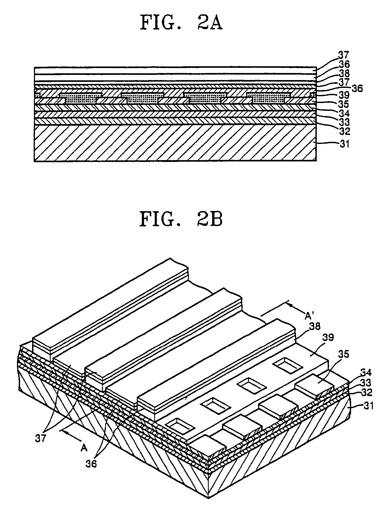
[0033]A perspective view of an organic EL device according to the present invention, which is a passive matrix, forward-emission display type, is shown in FIG. 2B. FIG. 2A is a sectional view of the organic EL device of FIG. 2B, taken along line A–A′.

[0034]Referring to FIGS. 2A and 2B, an organic EL device according to the first embodiment of the present invention includes a transparent glass substrate 31; a metal oxide layer 32, a thin metal layer 33, and a transparent spacer layer 34, which are sequentially deposited on the glass substrate 31; an indium tin oxide (ITO) anode layer 35 formed on the transparent spacer layer 34 as stripes; an inter-insulating layer 39 deposited on the transparent spacer layer 34 and the ITO anode layer 35 and patterned to expose a light emitting region of the ITO anode layer 35, as shown in FIG. 2B; an organic layer 36 on the inter-insulating layer 39; and a cathode layer 37 deposited on the organic layer 36 as a metallic total reflection layer. The ...

second embodiment

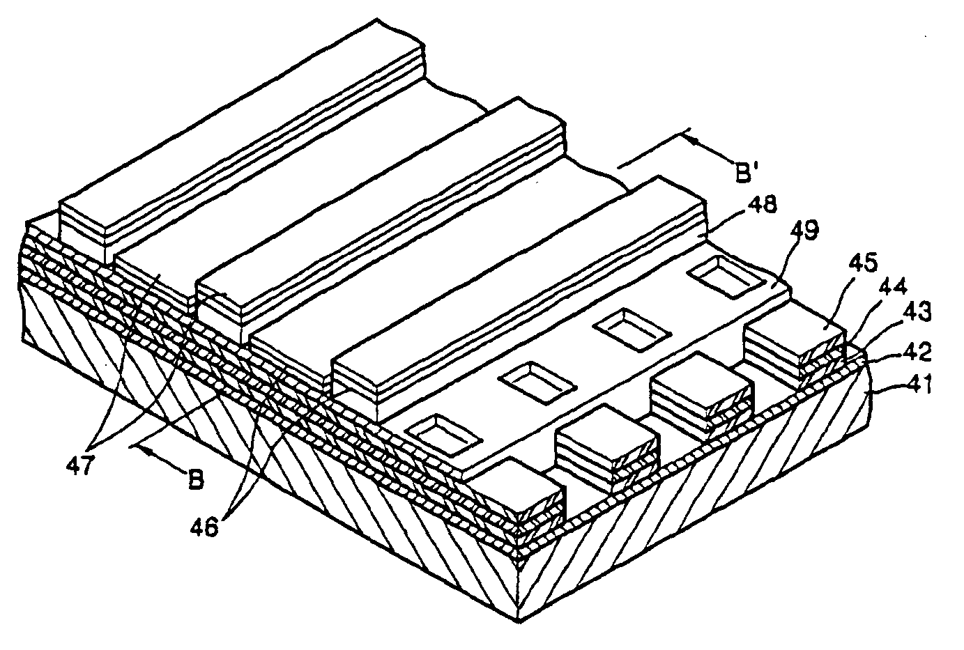
[0053]FIG. 3B is a perspective view of an organic EL device according to the present invention, and FIG. 3A is a sectional view of the organic EL device of FIG. 3B, taken along line B–B′.

[0054]Referring to FIGS. 3A and 3B, an organic EL device according to the second embodiment of the present invention includes: a transparent glass substrate 41; a metal oxide layer 42 deposited on the glass substrate 41; a thin metal layer 43, a transparent spacer layer 44, and an ITO anode layer 45, which are sequentially deposited on the metal anode layer 42 and patterned as stripes; an inter-insulating layer 49 deposited on the ITO anode layer 45 and the metal oxide layer 42 between the stripes of the ITO anode layer 45, the transparent spacer layer 44, and the thin metal layer 43 and patterned to expose a light-emitting region of the ITO anode layer 45; an organic layer 46 including an HIL contacting the exposed region of the ITO anode layer 45, a HTL, an EML, an ETL, and an EIL, which are seque...

third embodiment

[0060]In the organic EL device according to the present invention, the first ITO anode layer 55a instead of the transparent spacer layer 44(34) is formed underneath the thin metal layer 53, and the cathode layer 57, and the thickness of the first ITO anode layer 55a is controlled to manufacture a microcavity structure satisfying the requirements. When using an ITO anode, light transmittance slightly drops, compared with when using the transparent spacer layer 44(34), but may be considerably increased by appropriately controlling the thickness of the first ITO anode layer 55a.

[0061]The rectifying characteristics of the organic EL device, according to the third embodiment of the present invention, may degrade with an etching profile. To overcome this drawback, the first anode layer 55a underneath the thin metal layer 63 is removed in an organic EL device according to a fourth embodiment of the present invention.

[0062]FIG. 5 is a sectional view of an organic EL device according to the...


PUM


Abstract

An organic electroluminescent device induces optical resonance with a simple structure, the organic electroluminescent device including: a transparent substrate; a semi-transparent layer formed on the transparent substrate; a first anode layer formed on the semi-transparent layer as a predetermined pattern; a cathode layer formed of a metallic total reflection layer on the first anode layer; and an organic layer formed between the first anode layer and the cathode layer, which includes at least an emitting layer, wherein an optical distance between a top surface of the semi-transparent layer and a bottom of the cathode layer is determined to be a least integer multiple of half the peak wavelengths of light of a predetermined set of colors. Due to a resonance effect of the organic electroluminescent device, the emission efficiency of wavelengths of light of different colors is improved, and high-purity quality pictures may be displayed on the organic electroluminescent device.

Description

CROSS-REFERENCE TO RELATED APPLICATIONS[0001]This application claims priority from Korean Patent Application No. 2002-56813, filed on Sep. 18, 2002, in the Korean Intellectual Property Office, the disclosure of which is incorporated herein in its entirety by reference.BACKGROUND OF THE INVENTION[0002]1. Field of the Invention[0003]The present invention relates to an organic electroluminescent device, and more particularly, to an organic electroluminescent device using an optical resonance effect.[0004]2. Description of the Related Art[0005]Electroluminescent (EL) display devices may be classified into inorganic and organic devices depending on the material composing their emitter layers.[0006]In organic EL devices, externally injected electrons and holes combine in an emitter layer and dissipate to generate excitons. As these excitons transit from an excited state to a base state, energy is transferred to fluorescent molecules in the emitter layer, enabling the molecules to emit lig...

Claims


Application Information

Patent Timeline
Patent Type & Authority Patents(United States)
IPC IPC(8): H05B33/22G02B5/26G02B5/28H01L27/32H01L51/50H05B33/24H05B33/26
CPCH01L51/5265H01L27/3281H01L27/3295H10K59/17H10K59/173H10K50/852H05B33/22
Inventor LIM, JUNG KUNAM, WI JIN
Owner SAMSUNG DISPLAY CO LTD
Why Eureka
Try Eureka