
Radio frequency power amplifier and communication system

a technology of radio frequency and power amplifier, which is applied in the direction of amplifiers, amplifiers with semiconductor devices only, amplifiers with semiconductor devices, etc., can solve the problems of increasing signal distortion, and achieve the effects of suppressing envelope waveform distortion, reducing gain, and high efficiency

Inactive Publication Date: 2006-08-29
RENESAS TECH CORP
View PDF8 Cites 10 Cited by
  • Summary
  • Abstract
  • Description
  • Claims
  • Application Information

AI Technical Summary

Benefits of technology

[0006]Let us consider a case where the above-mentioned high-frequency power amplifier according to the prior art employs an SiGe HBT instead of a GaAs HBT as the amplifying transistor. The SiGe HBT contains a base comprising SiGe mix crystal and an emitter and a collector comprising Si. In such case, the following advantages and problems occur due to a difference between GaAs HBT and SiGe HBT characteristics.
[0007]The SiGe HBT reduces an emitter resistance per emitter area to 1 / 40 to 1 / 20 of that for the GaAs HBT. Accordingly, the SiGe HBT has advantages of decreasing a loss in the emitter resistor and improving the efficiency during a power amplification operation. However, there is a side effect of increasing signal distortion due to the amplification. This is because a small emitter resistance causes remarkable exponential relationship between voltage and current characteristics. Further, the input / output relationship becomes more non-linear.

Problems solved by technology

However, there is a side effect of increasing signal distortion due to the amplification.

Method used


Image

  • Radio frequency power amplifier and communication system
  • Radio frequency power amplifier and communication system
  • Radio frequency power amplifier and communication system

Examples


embodiment 1

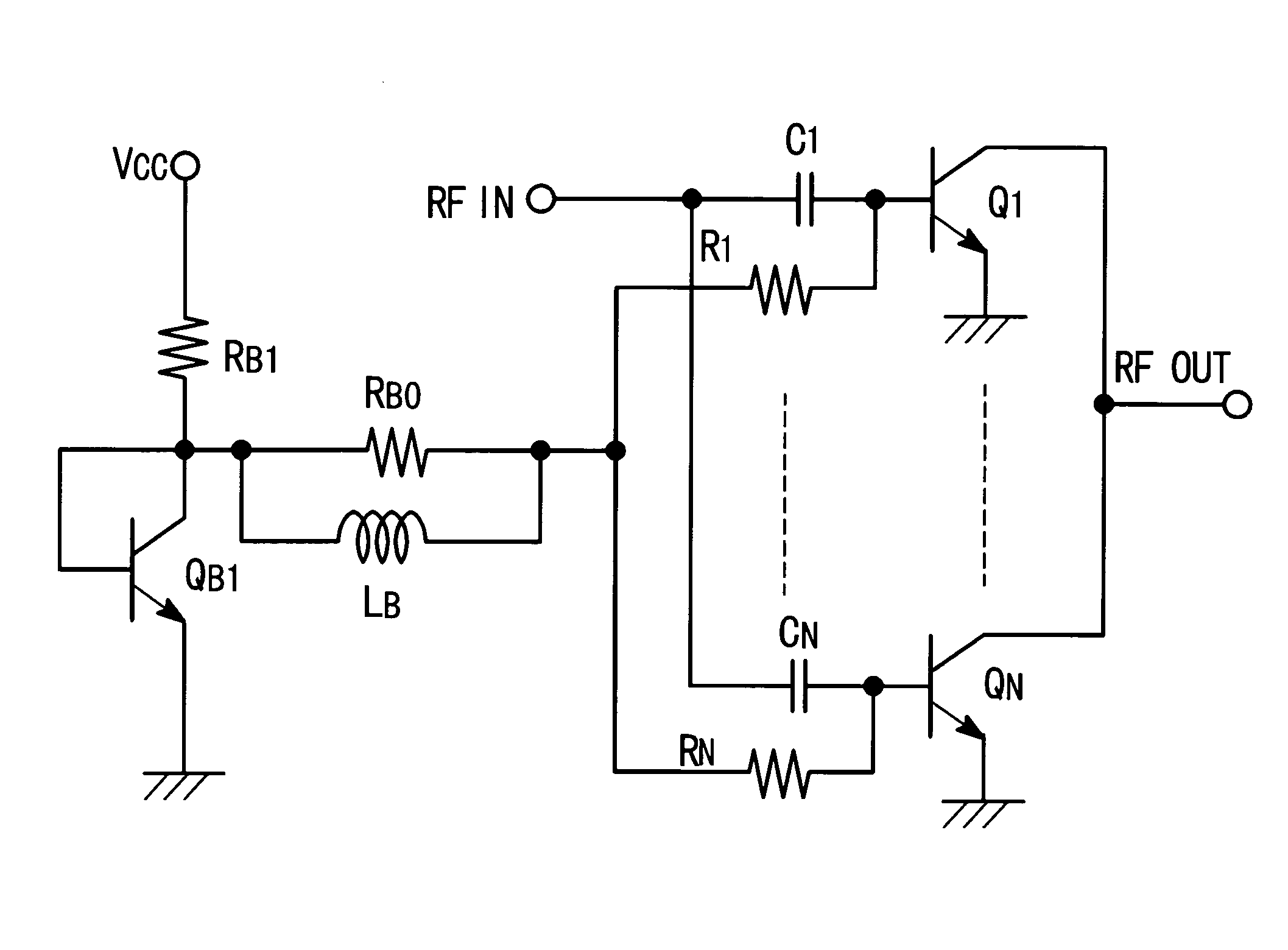
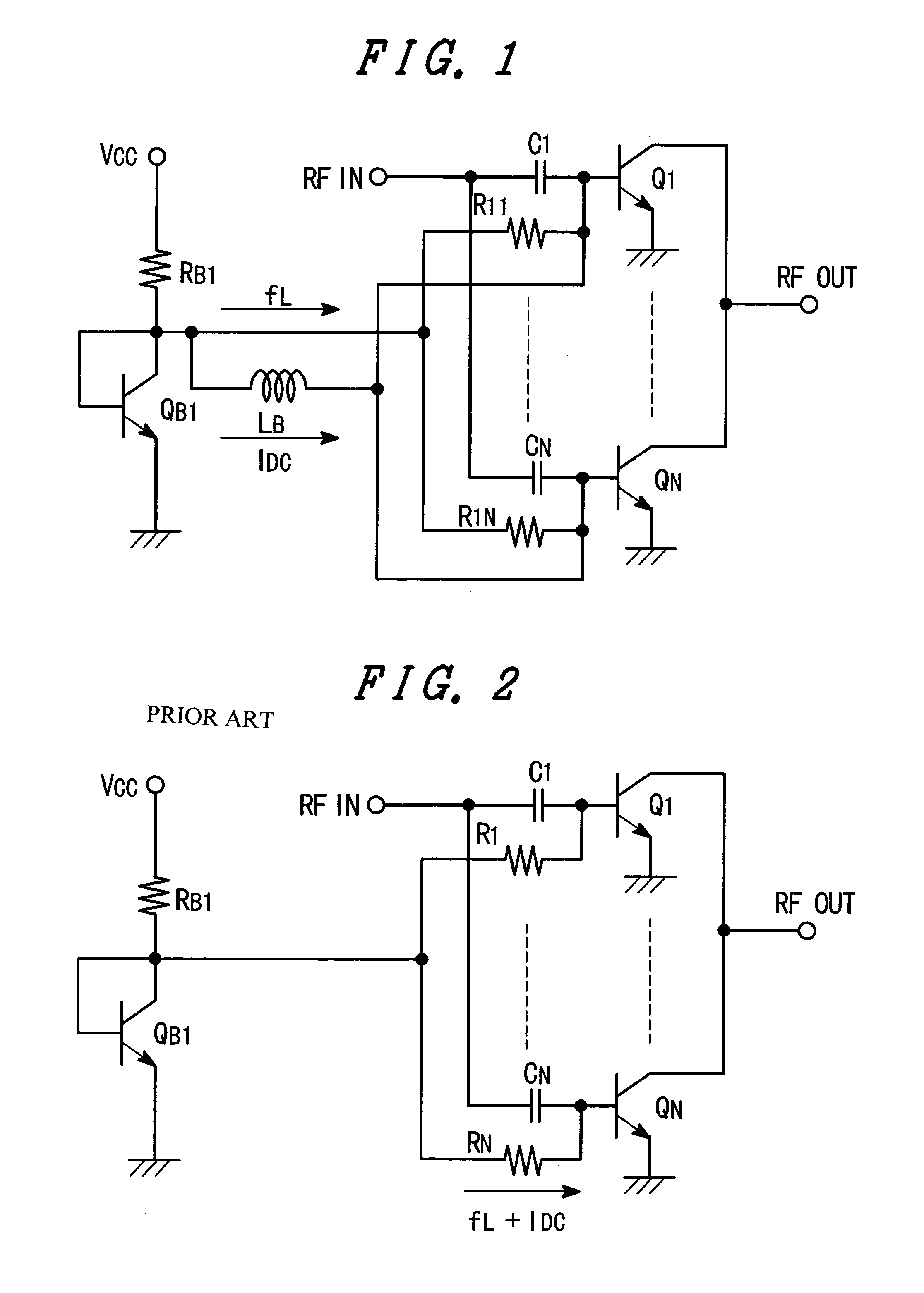
[0056]FIG. 1 is a circuit diagram showing a major part of a radio frequency power amplifier compliant with WCDMA (Wide-band Code Division Multiple Access) indicative of the first embodiment of the present invention. The diagram includes an amplifying transistor and a bias circuit connected to its base.

[0057]The embodiment exemplifies a combination of the fist means and the first configuration of the second means. This example shows arrangement of a coil parallel to a bias resistor having a value three to five times greater than that of a conventional ballast resistor.

[0058]In FIG. 1, the reference symbols Q1 to QN denote N equivalent SiGe HBTs; C1 to CN denote N equivalent capacitors; R11 to R1N denote N equivalent resistors; QB1 denotes an SiGe HBT; RB1 denotes a resistor; LB denotes a coil; VCC denotes a constant voltage supply; RFin denotes a high-frequency input terminal; and RFout denotes a high-frequency output terminal. The term “equivalent” here signifies an attribute of hav...

embodiment 2

[0064]FIG. 4 is a circuit diagram showing a major part of a WCDMA compliant radio frequency power amplifier according to the second embodiment of the present invention. The diagram includes an amplifying transistor and a bias circuit connected to its base. FIG. 4 uses the same reference symbols as those for the conventional example and the first embodiment shown in FIG. 2 and a detailed description is omitted for convenience of description.

[0065]According to the embodiment, wiring from each base of the transistors Q1 through QN branches into two paths. Like the conventional example in FIG. 2, one of the paths unites with the corresponding wiring of the other transistors via one of capacitors C1 through CN and is connected to the high-frequency input terminal. The other path unites with the corresponding wiring of the other transistors via one of ballast resistors R1 through RN. Unlike the first embodiment, this path is further connected to the collector of the transistor QB1 via the...

embodiment 3

[0068]FIG. 5 is a circuit diagram showing a major part of a WCDMA compliant radio frequency power amplifier according to the third embodiment of the present invention. The diagram includes an amplifying transistor and a bias circuit connected to its base.

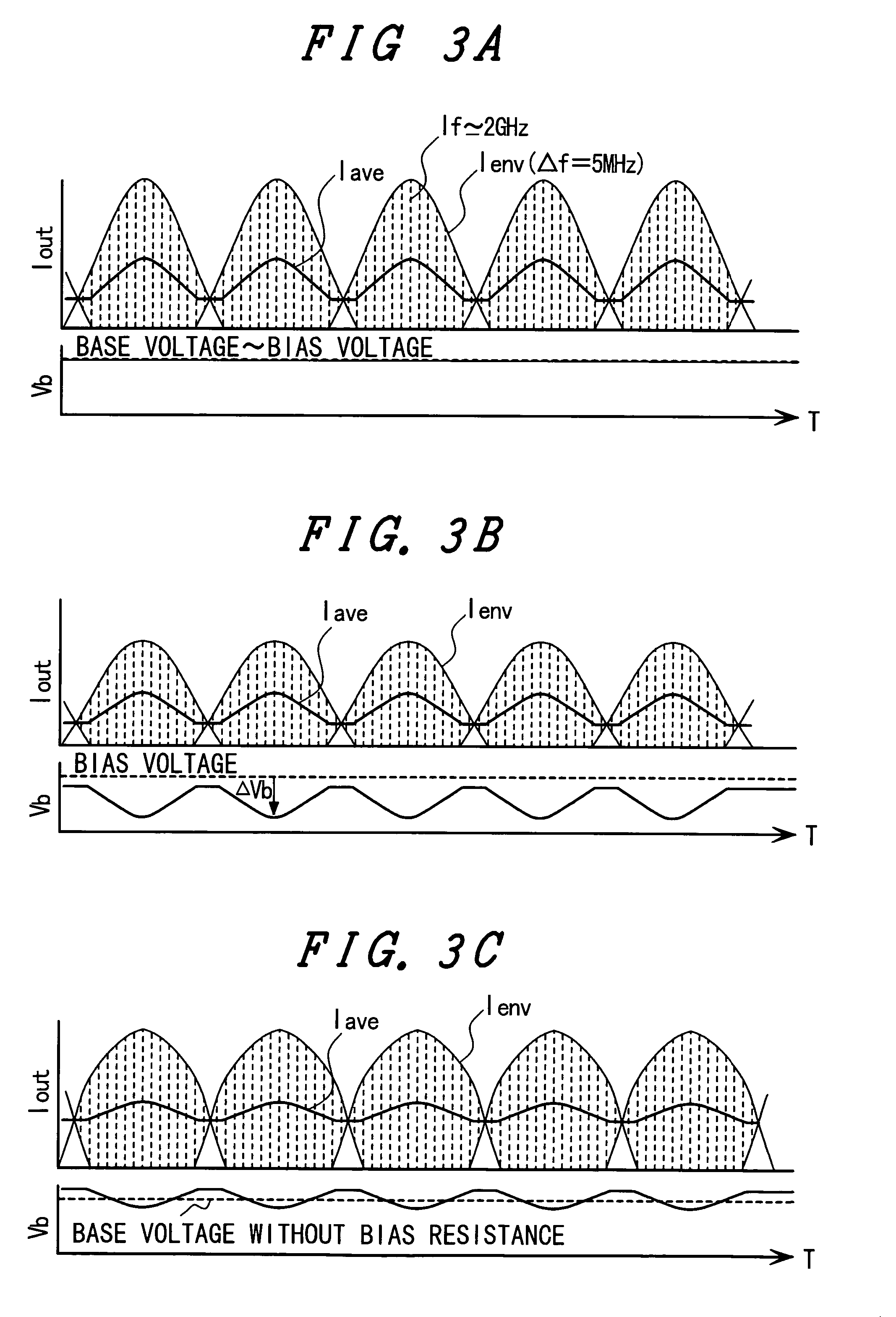
[0069]The third to eighth embodiments are combinations of the first means and the second configuration of the second means and provide specific configuration examples for realizing the following function. That is to say, there is provided a bias resistor having a value three to five times greater than that of a conventional ballast resistor. The function detects the amount of decrease in the amplifying transistor's base average voltage due to a voltage drop in the bias resistor. The function automatically increases an output voltage from the base bias circuit so as to compensate this voltage drop. These embodiments have the basic common configuration that comprises circuit components including at least one bipolar transistor configu...


PUM


Abstract

There is provided not only a radio frequency power amplifier using an SiGe HBT subject to a little amplification distortion, but also a communication system using the same. A conventional radio frequency power amplifier provides base bias paths of transistors Q1 through QN (SiGe HBT) with bias resistors R11 through R1N having resistance values three to five times higher than those of a ballast resistor attached to each transistor's base. A coil LB is provided in parallel with the bias resistor as a means for compensating a voltage drop due to direct current component IDC flowing through the bias resistor. Addition of the bias resistor suppresses non-linearity of low-frequency variations in an output current. Addition of the coil compensates for voltage drop. Accordingly, the maximum linear output power can be improved. As a result, it is possible to provide the power amplifier subject to a little amplification distortion within a wide output range.

Description

FIELD OF THE INVENTION[0001]The present invention relates to a radio frequency power amplifier and a wireless communication terminal such as a cellular phone and the like using the same.BACKGROUND OF THE INVENTION[0002]Conventionally, a configuration in FIG. 2 is widely known as such type of radio frequency power amplifier (see patent document 1). There is used a plurality of GaAs Hetero-junction Bipolar Transistors (Q1 through QN) as high-frequency amplifying transistors. The hetero-junction bipolar transistor is hereinafter referred to as HBT or simply as a transistor.[0003]As shown in FIG. 2, an emitter of each transistor (Q1 through QN) is grounded. A base connects with a high-frequency input terminal via a capacitor (C1 through CN). A collector connects with a high-frequency output terminal. The base of each transistor is connected to a base bias circuit via a resistor (R1 through RN). The base bias circuit comprises an HBT (QB1) and a resistor RB1. An emitter of the transistor...

Claims


Application Information

Patent Timeline
Patent Type & Authority Patents(United States)
IPC IPC(8): H03F3/68H03F1/32H03F1/30H03F3/21
CPCH03F1/302H03F3/211H03F2203/21178H03F2200/372
Inventor KONDO, MASAOMASUDA, TORUWASHIO, KATSUYOSHI
Owner RENESAS TECH CORP
Learn More