Image sensor with stabilized black level and low power consumption

a black level and image sensor technology, applied in the field of image sensors, can solve the problems of lateral stripe noise, increased chip area, and increased cost, and achieve the effect of preventing variations in black level

Inactive Publication Date: 2006-08-29
SOCIONEXT INC
View PDF6 Cites 46 Cited by
  • Summary
  • Abstract
  • Description
  • Claims
  • Application Information

AI Technical Summary

Benefits of technology

[0015]Accordingly, it is an object of the present invention to provide an image sensor capable of preventing variations in black level due to a pixel defect.
[0016]It is another object of the present invention to provide an image sensor capable of obtaining a black clamp level in a shorter time.
[0017]It is still another object of the present invention to provide an image sensor capable of decreasing power consumption by performing fine on / off control of a power source for an internal circuit in a case of a reduced frame rate.
[0019]With this aspect, a potential averaging processing is automatically performed before reading out a signal from the optical black pixel region instead of performing an averaging processing in a black clamp circuit as in the prior art. Therefore, a black level (integrated dark current signal) is stabilized, more correct line black clamp is performed, and lateral stripe noise is reduced, thereby improving an image quality.
[0021]Furthermore, since a black clamp level (an offset value) can be obtained in a shorter time than in the prior art because of the above described reason, there is no problem even if quite many pixels exist in a pixel array and thereby a blanking period is short.
[0023]With this aspect, power supply for the read-out circuit ceases in the light integration period and besides, power supply to the pixel array and the read-out circuit ceases in the power-off period, thereby power consumption in the image sensor can be reduced.

Problems solved by technology

Especially, when a defective pixel exists, an integrated dark current signal suddenly changes as shown in FIG. 19, therefore an offset value becomes incorrect in a black clamp circuit having a integration capacitor for obtaining an average value, which causes lateral stripe noise.
If the width of the optical black pixel region is wide in order to prevent the noise, the offset component could not be obtained in a horizontal blanking period in an image sensor having quite many pixels, or a chip area increases with the result of higher cost.
However, the chip of an image sensor includes an analogue circuit and a digital circuit, power consumption of the analog circuit is larger than that of the digital circuit with a large ratio, and power consumption of an image sensor for taking a moving picture cannot decrease to a great extent by such methods.
When a power source for the analog circuit is on / off controlled, the influence of off appears after one frame, therefore the power source cannot be simply turned off.

Method used


Image

  • Image sensor with stabilized black level and low power consumption
  • Image sensor with stabilized black level and low power consumption
  • Image sensor with stabilized black level and low power consumption

Examples


first embodiment

[0045

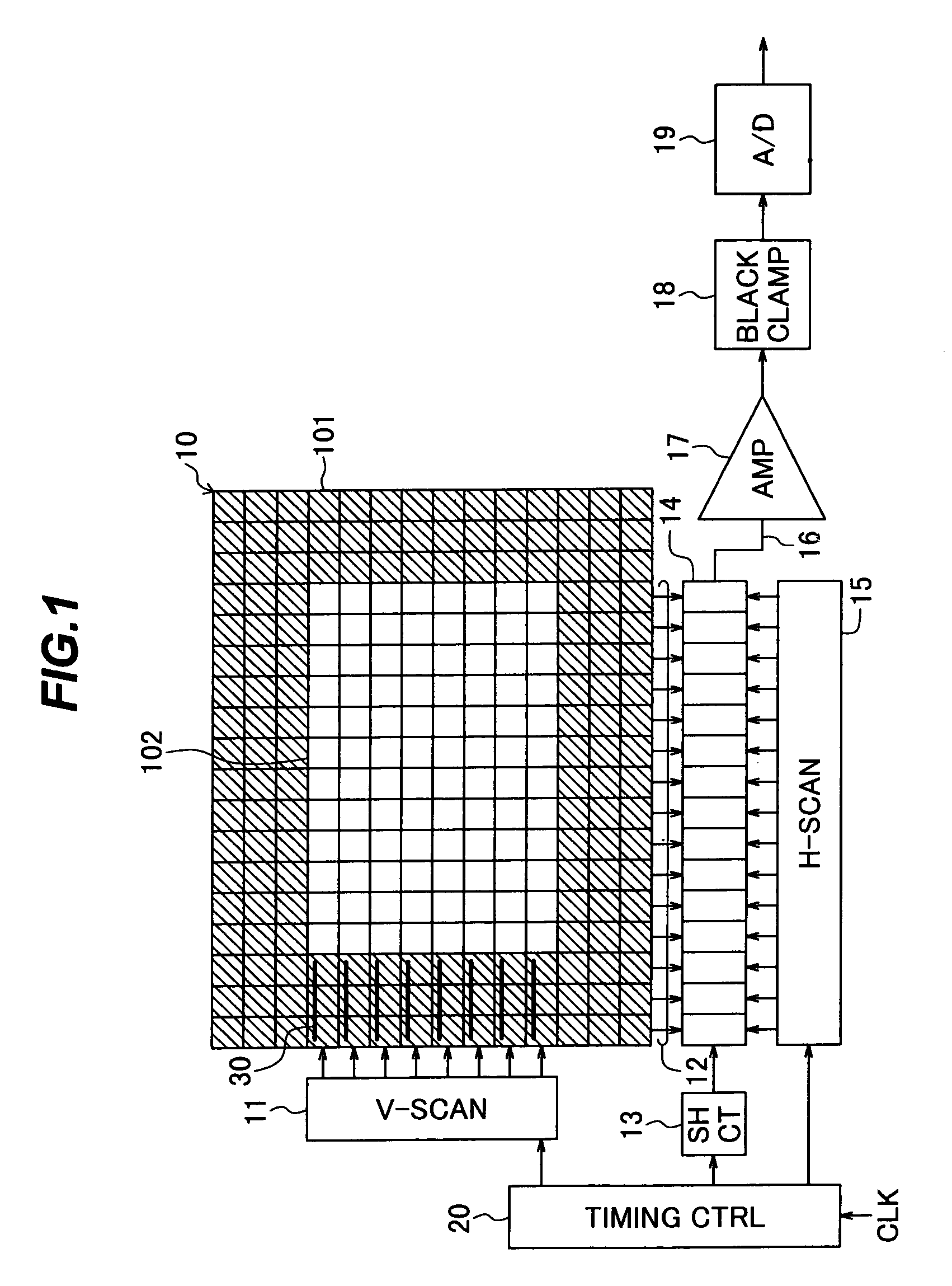
[0046]FIG. 1 is a schematic block diagram showing an image sensor of a first embodiment according to the present invention.

[0047]The image sensor is, for example, of a MOS type.

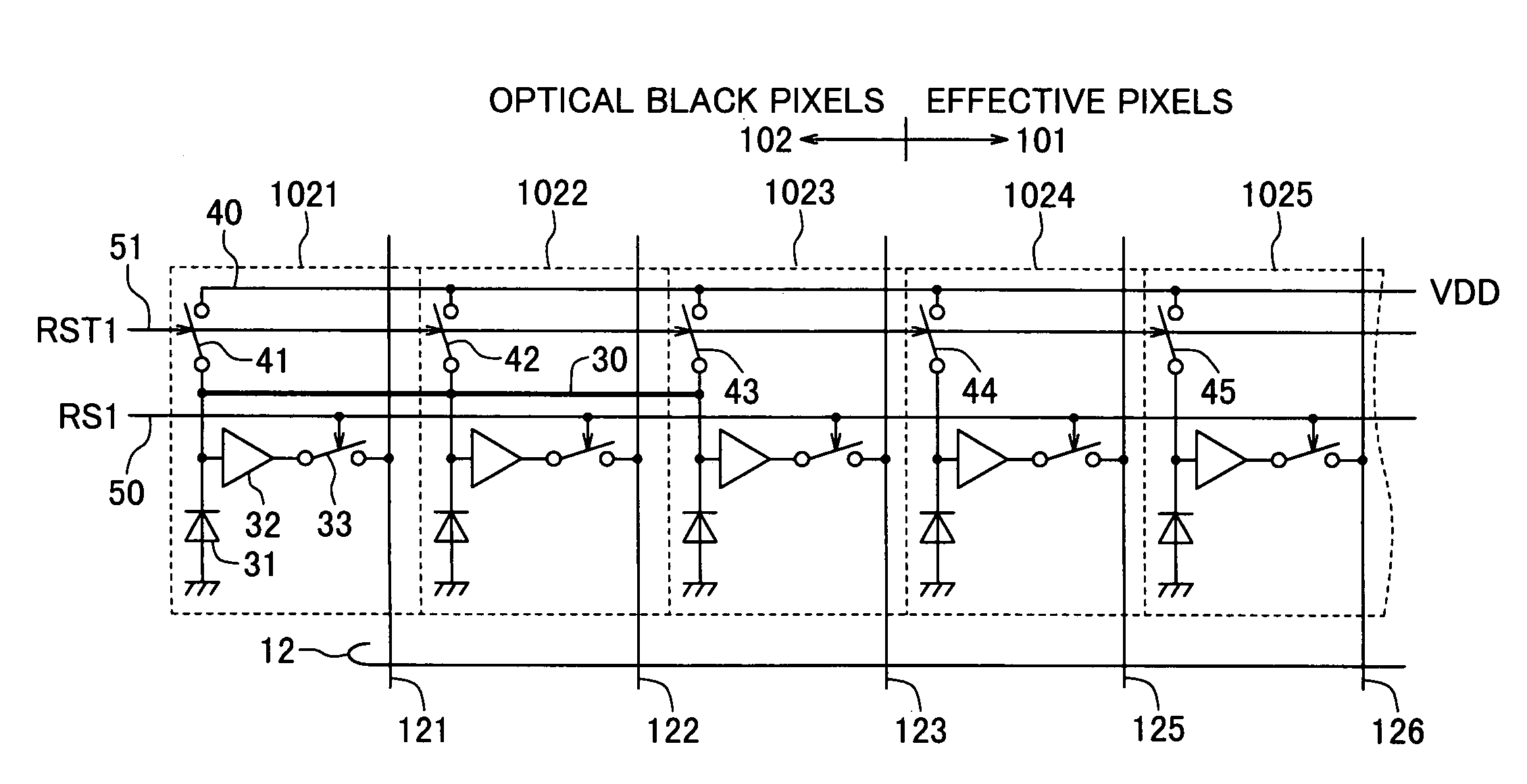
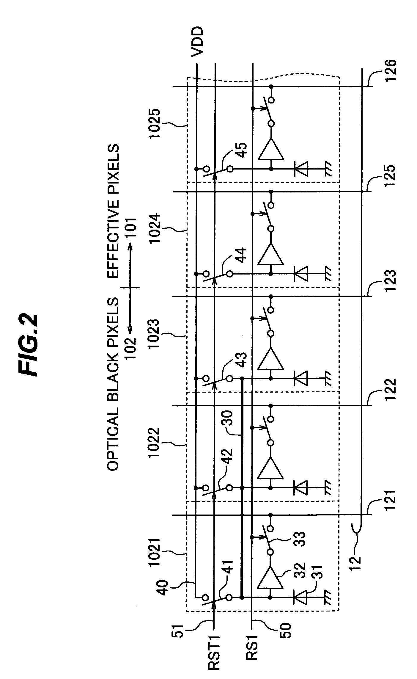
[0048]A pixel array 10 has pixels arranged in rows and columns. The hatched peripheral portion in the pixel array 10 is an optical black pixel region 101 in which light receiving elements are covered with a light shielding film such as an aluminum film. Since light can not enter into the light receiving elements in the optical black pixel region 101, only an integrated dark current signal is read out from this region. An area inside the optical black pixel region 101 is an effective pixel region 102 with no light shielding film thereon.

[0049]In the horizontal scanning start side of the optical black pixel region 101 and beneath the light shielding film, potential averaging lines 30 drawn with thick lines in FIG. 1 are formed along pixel rows.

[0050]Pixels of the optical black pixel region 101 are the same...

second embodiment

[0065

[0066]FIG. 4 is a schematic block diagram showing an image sensor of a second embodiment according to the present invention.

[0067]In this image sensor, among the vertical bus lines in the optical black pixel region 101, only the vertical line 123 of FIG. 2 is connected to the signal input of one of sample and hold circuits 14A.

[0068]Thereby, even when the number of pixels in the pixel array 10 is quite large and in turn the horizontal blanking period is short, the black clamp level can be correctly sampled by the black clamp circuit 18 in this short period.

[0069]Further, the number of the sample and hold circuits 14A and stages of a horizontal scanning circuits 15A can be smaller than that in the case of FIG. 1.

[0070]The other points are the same as that of the first embodiment.

third embodiment

[0071

[0072]FIG. 5 is a schematic block diagram showing an image sensor of a third embodiment according to the present invention.

[0073]In this image sensor, a mode signal MODE is provided to a horizontal scanning circuit 15B. The circuit 15B scans from the left side to the right side in FIG. 5 when the mode signal MODE indicates a normal image mode, and scans in the opposite direction when the mode signal MODE indicates a left / right reverse image mode (or a top / bottom and left / right reverse image mode).

[0074]The black clamp level for each horizontal line is necessary to be determined prior to scanning effective pixels on the same line, potential averaging lines drawn with thick lines are formed on the both sides of the horizontal scanning lines. In each of the both sides, one vertical bus line is connected to the signal input of end one of the sample and hold circuit 14B.

[0075]The other points are the same as that of the second embodiment.


PUM


Abstract

The control inputs of reset switch elements 41 to 45 are commonly connected to a row reset line 51. In a line black clamp type, cathodes as reset ends of photodiodes (31) of optical black pixels 21 to 23 are commonly connected to a potential averaging line 30. In a frame black clamp type, potential averaging lines are connected similarly to respective pixel rows on the vertical scanning start side of an optical black pixel region, and the potential averaging lines may be commonly connected to each other to operate just like one pixel row. A first block includes a pixel array and a vertical scanning circuit, while a second block includes sample and hold circuits, a horizontal scanning circuit, an amplifier and an A / D converter 19. In a low power consumption mode, power supply to the second block is ceased in a light integration period of one frame with performing light integration in the pixel array, power supply to the first and second blocks is performed in a read-out period of one frame to read out integrated signals, and power supply to the first and second blocks is ceased in a power-off period of one frame.

Description

BACKGROUND OF THE INVENTION[0001]1. Field of the Invention[0002]The present invention relates generally to an image sensor, more particularly, to an image sensor having plurality of pixels arranged in rows and columns, for use in such an electronic camera, an image reader or a facsimile, with a stabilized black level and low power consumption.[0003]2. Description of the Related Art[0004]In an image sensor, each light receiving element outputs a signal having an integrated light component and an integrated dark current component. This dark current has a strong temperature dependency that the current becomes about twice with rise of 9° C.[0005]In order to remove the integrated dark current component from the signal to obtain true integrated light signal, in the prior art, the peripheral region of a pixel array was covered with a light shielding film to form an optical black pixel region, and an integrated dark current signal was read out from the optical black pixels in a blanking per...

Claims


Application Information

Patent Timeline
Patent Type & Authority Patents(United States)
IPC IPC(8): H04N9/64H04N5/361H04N5/3745
CPCH04N5/23241H04N5/3745H04N5/361H04N23/651H04N25/633H04N25/63H04N25/77
Inventor YAMAMOTO, KATSUYOSIFUNAKOSHI, JUN
Owner SOCIONEXT INC
Why Eureka
Try Eureka