Semiconductor device and manufacturing method for the same

a technology of semiconductors and semiconductors, applied in the direction of semiconductor devices, basic electric elements, electrical appliances, etc., can solve the problems of low main withstand voltage, low on resistance, and large drop in main withstand voltage,

Inactive Publication Date: 2006-09-12
MITSUBISHI ELECTRIC CORP
View PDF18 Cites 16 Cited by
  • Summary
  • Abstract
  • Description
  • Claims
  • Application Information

AI Technical Summary

Benefits of technology

[0042]An object of the present invention is to provide a structure which improves the trade-off relationship between the main withstanding voltage and the ON resistance, and a manufacturing method capable of implementing such a structure in a semiconductor device based on a three-dimensional multiple RESURF effect.

Problems solved by technology

In an actual element, however, this repeating microscopic structure of p-type and n-type layers cannot be repeated infinitely in an edge portion of the chip and, therefore, there is a problem wherein a drop in the main withstand voltage is great in a “termination” portion of a termination structure where the repetition ends.
Therefore, though the element operates, there is a problem wherein the trade-off relationship between the main withstand voltage and the ON resistance does not improve.
According to this technique, however, there is a problem wherein implementation is difficult due to the reasons described below.
However, a p− region cannot actually be formed to have such a concentration distribution.
There is a problem, however, wherein the original effects of Prior Art 1 cannot easily be exercised when the formula for the relationship of the pn concentration ratio is not fulfilled in the case that the absolute values of the concentration greatly change or when the description of such a relationship becomes extremely complex so that the precision of proximity is reduced.
First, concentration regulation for forming an SJT structure is too complicated and it is necessary to apply an interval design that agrees with the concentration arrangement of the repeating cell portions that are different from the termination structure portions to the SJT part after examining the arrangement in detail before carrying out the actual design and, in addition, it is physically and mechanically difficult to fabricate a semiconductor chip structure to include terminal edges. On the other hand, the present invention has the advantage that both design and manufacturing method are simple because the relative concentrations in the vicinity of the terminal edges of the repeating cell portions may be adjusted using comparatively simple arithmetic.
Secondly, an SJT structure can only be implemented in the case of manufacture by means of a buried multi-layer epitaxial growth method and lacks versatility in that it cannot be actually manufactured in the case wherein a trench sidewall diffusion is used.
Furthermore, as described in the main body of Prior Art 1, there is a problem wherein this technique lacks versatility in that it is impossible to apply this technique in an element structure wherein a trench system is applied due to restrictions of the manufacturing technology even though the application to a multi-layer epitaxial structure is, in principle, possible.
Therefore, in the same manner as in the above described Prior Art 1, the difference in the electrical field distribution between the inside of repeating cells and the termination structure portions becomes greater so that there is a problem wherein a high withstand voltage, which is essentially obtained in a cell portion, cannot be implemented although the relationship between the main withstanding voltage and the ON resistance is improved in comparison with the conventional MOS-FET structure.

Method used


Image

  • Semiconductor device and manufacturing method for the same
  • Semiconductor device and manufacturing method for the same
  • Semiconductor device and manufacturing method for the same

Examples


first embodiment

[0200](First Embodiment)

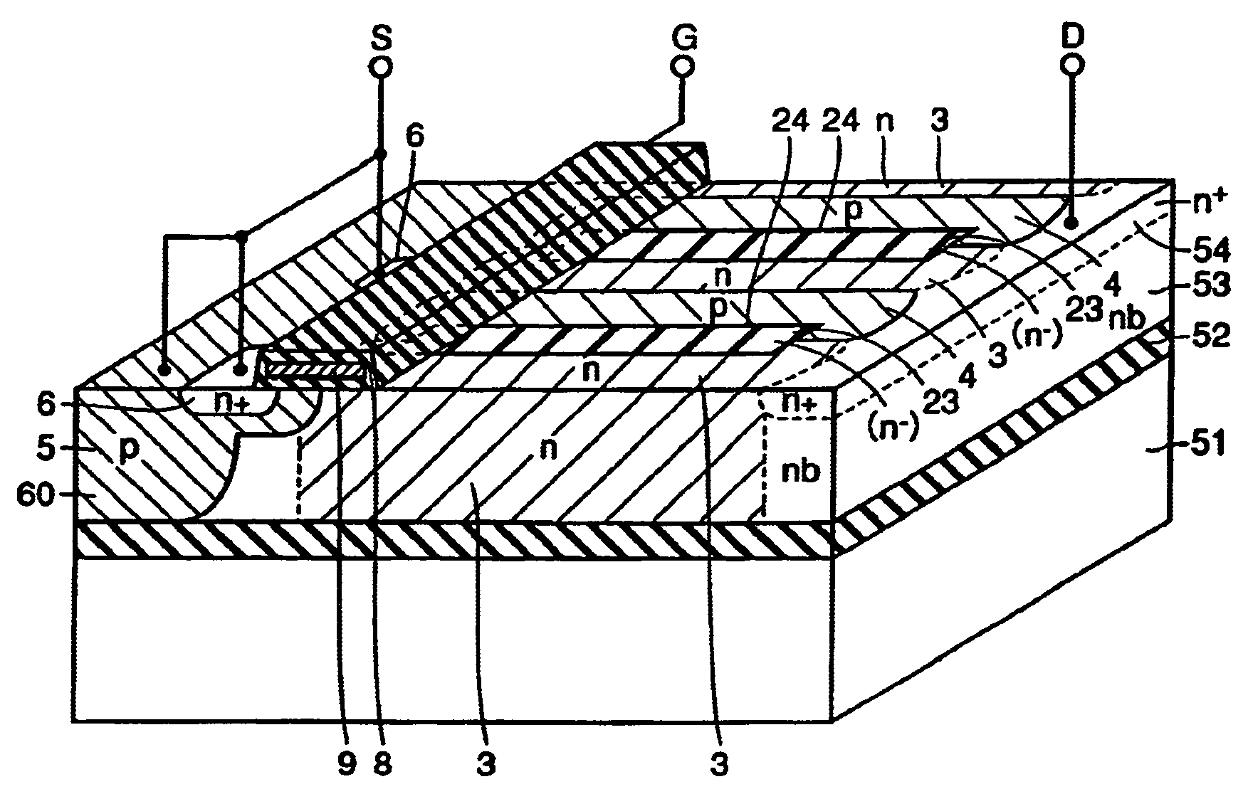
[0201]FIG. 1 shows a configuration that corresponds to the case wherein a MOS-FET is posited as a concrete active element structure. In reference to FIG. 1, an n− epitaxial layer 2 is formed on the first main surface side of an n+ drain region 1 of the MOS-FET. A pn-repeating structure is formed within this n− epitaxial layer 2 wherein n-type drift regions 3 and p-type impurity regions 4 are repeated in alternation.

[0202]Here, the vicinity of the center of the element having this pn-repeating structure is omitted for simplification of explanation and the pitch of pn repetition is approximately 1 μm to 20 μm and, therefore, several hundreds to several tens of thousands of pairs of n-type drift regions 3 and p-type impurity regions 4 usually exist in the form of repeated combinations in this portion. The n-type impurity concentration of an n-type drift region 3 and the p-type impurity concentration of a p-type impurity region 4, which are combined in a pair, ar...

second embodiment

[0221](Second Embodiment)

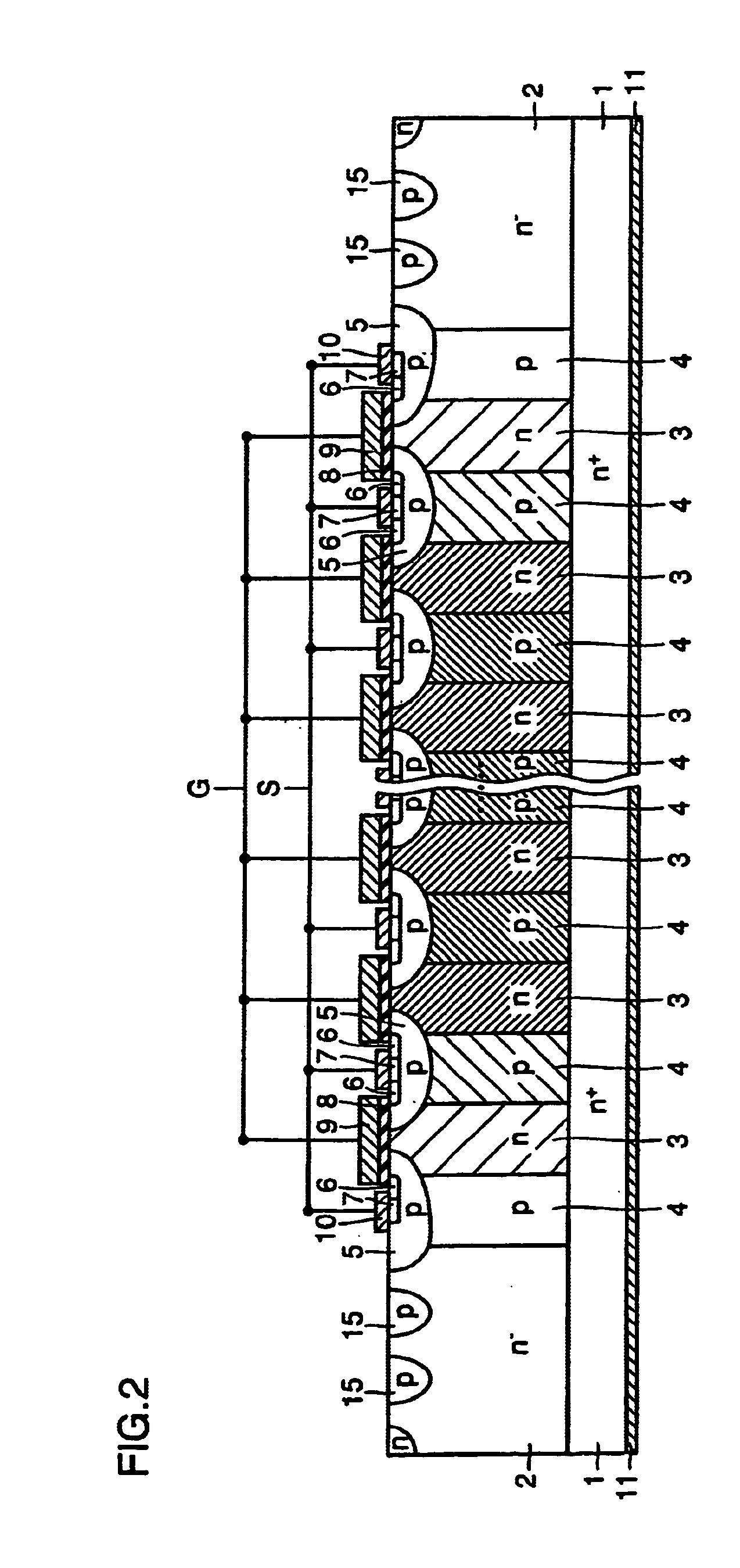
[0222]In reference to FIG. 2, the configuration of the present invention differs from the configuration shown in FIG. 1 in the point that the present embodiment has a configuration wherein the concentrations of n-type drift regions 3 and p-type impurity regions 4 are independently lowered to get lesser in an alternating manner in the direction toward the edge portion side in four stages without using each combination of n-type drift region 3 and p-type impurity region 4 (hereinafter referred to as a pn combination) as one unit. That is to say, p-type impurity region 4 located at the outermost portion of the pn-repeating structure is a region of extremely low concentration having the lowest impurity concentration. n-type drift region 3 adjoining this p-type impurity region 4 at the outermost portion is a low concentration region having the next lowest impurity concentration. p-type impurity region 4 adjoining this n-type drift region 3 on the center portion s...

third embodiment

[0228](Third Embodiment)

[0229]In reference to FIG. 3, the configuration of the present embodiment differs from the configuration of the first embodiment in the point wherein the low concentration region at the outermost portion of the pn-repeating structure in the configuration of the present embodiment is formed of only one pair of the pn combination, which is one unit. That is to say, the pair formed of the pn combination 3 and 4 located at the outermost portion of the pn-repeating structure has the same impurity concentration and has an impurity concentration lower than that of the high concentration regions 3 and 4 in the center portion.

[0230]In addition, as for the concentration setting of the respective regions in the case that the concentration gradient has only one stage, as in the present embodiment, the impurity concentration of each of the low concentration regions 3 and 4 is preferably no less than 30% and no greater than 70% in the case that the impurity concentration o...


PUM


Abstract

A semiconductor device of the present invention has a pn-repeating structure that a structure in which a p-type impurity region (4) and an n-type drift region (3) are aligned side by side is repeated twice or more, and a low concentration region which is either p-type impurity region (4) or n-type drift region (3) located at the outermost portion of this pn-repeating structure has the lowest impurity concentration or has the least generally effective charge amount among all the p-type impurity regions (4) and n-type drift regions (3) forming the pn-repeating structure.Thereby, the main withstand voltage of a power semiconductor device to which a three dimensional multi-RESURF principle is applied, wherein the element withstand voltage is specifically in the broad range of 20 to 6000 V, can be improved and the trade-off relationship between the main withstand voltage and the ON resistance can also be improved, so that an inexpensive semiconductor device of which the power loss is small and of which the size of the chip is small can be obtained.In addition, a trench of a dotted line trench (DLT) structure and a manufacturing method corresponding to this can be used, so that a semiconductor device with a good yield can be obtained at low cost.

Description

[0001]This application is a divisional of application Ser. No. 10 / 257,775 filed Oct. 17, 2002 now U.S. Pat. No. 6,821,824.TECHNICAL FIELD[0002]The present invention relates to a semiconductor device and a manufacturing method for the same, and more particularly to an improvement in performance and an increase in the yield of a power semiconductor device.BACKGROUND ART[0003]An element using a repeating microscopic structure of p-type and n-type layers wherein an electric field relaxation phenomenon called the RESURF (REduced SURface Field) effect is applied in place of the uniform n-type drift layer of a conventional MOS-FET (Metal Oxide Semiconductor-Field Effect Transistor) has been proposed in, for example, U.S. Pat. No. 6,040,600. In this element a low ON resistance is obtained in the ON condition due to the n-type drift layer of which the impurity concentration is higher than the concentration of the uniform n drift layer in the conventional structure by approximately one order ...

Claims


Application Information

Patent Timeline
Patent Type & Authority Patents(United States)
IPC IPC(8): H01L21/332H01L21/265H01L21/266H01L21/336H01L29/06H01L29/78
CPCH01L29/0619H01L29/0634H01L29/0649H01L29/0834H01L29/66712H01L29/7801H01L29/7802H01L29/7824H01L29/0653H01L21/26586H01L21/266H01L29/7823H01L29/7811H01L21/18
Inventor MINATO, TADAHARUNITTA, TETSUYA
Owner MITSUBISHI ELECTRIC CORP
Why Eureka
Try Eureka