Self-aligned trench DMOS transistor structure and its manufacturing methods

a self-aligned, trench-type technology, applied in the direction of basic electric elements, electrical equipment, semiconductor devices, etc., can solve the problems of slow switching speed, improve the ruggedness of trench-type dmos transistors, improve the parasitic gate-interconnection resistance, and improve source and p-base contact resistance.

Inactive Publication Date: 2006-09-19
SILICON BASED TECH
View PDF2 Cites 63 Cited by
  • Summary
  • Abstract
  • Description
  • Claims
  • Application Information

AI Technical Summary

Problems solved by technology

Moreover, the parasitic resistance of the doped polycrystalline-silicon layer 114 as a gate metal layer is very large for gate interconnection of many trench DMOS transistor cells and may result in a slower switching speed.

Method used


Image

  • Self-aligned trench DMOS transistor structure and its manufacturing methods
  • Self-aligned trench DMOS transistor structure and its manufacturing methods
  • Self-aligned trench DMOS transistor structure and its manufacturing methods

Examples


first embodiment

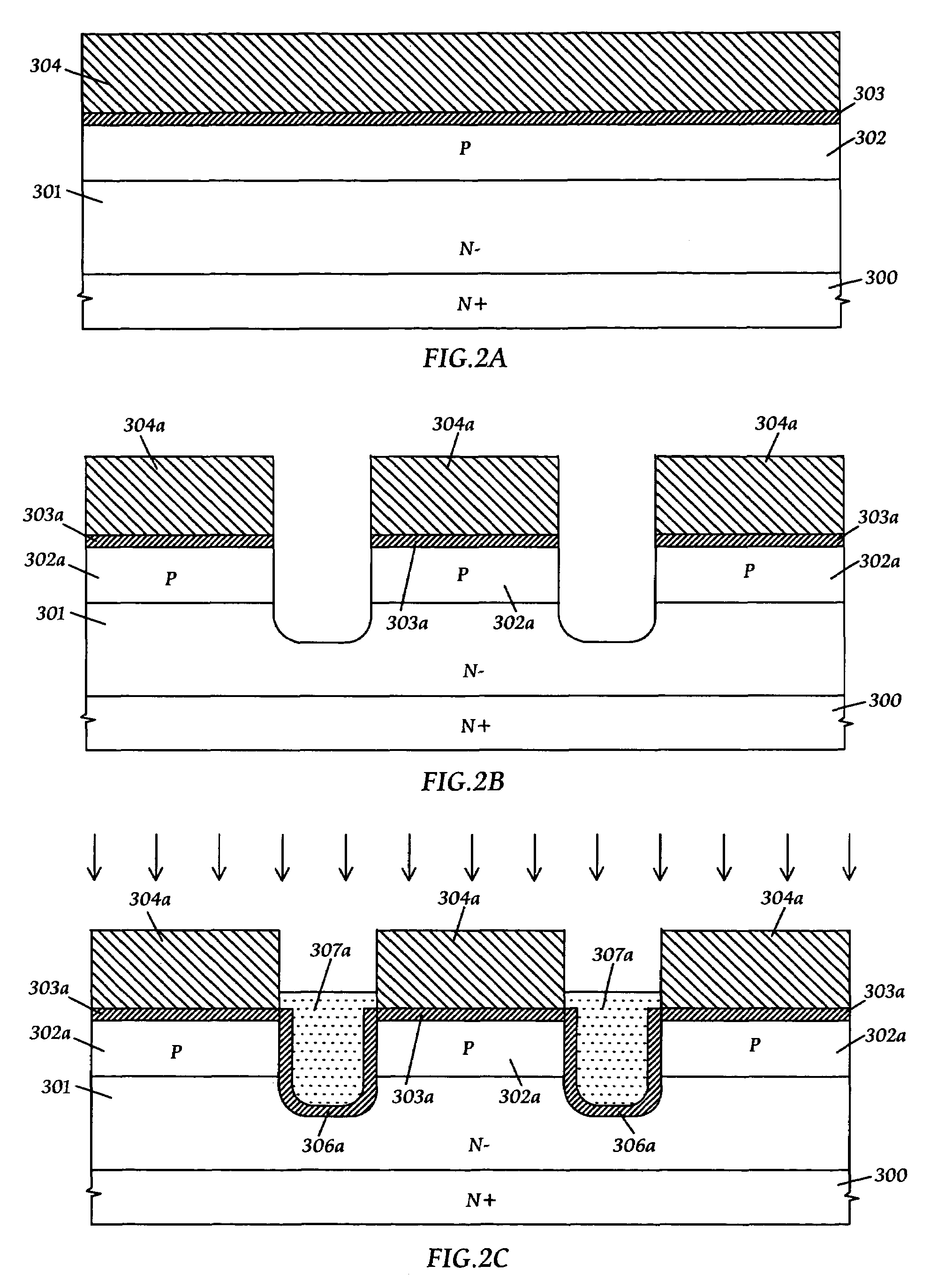
[0018]Referring now to FIG. 2A through FIG. 2J, there are shown process steps and their schematic cross-sectional views of fabricating a self-aligned trench DMOS transistor structure for the present invention.

[0019]FIG. 2A shows that a p-diffusion region 302 is formed in an epitaxial silicon substrate 301 / 300 with an N− epitaxial silicon layer 301 being formed on an N+ silicon substrate 300; a buffer oxide layer 303 is then formed on the p-diffusion region 302; and thereafter, a masking dielectic layer 304 is formed on the buffer oxide layer 303. The masking dielectric layer 304 is preferably made of silicon nitride as deposited by low pressure chemical vapor deposition (LPCVD). The buffer oxide layer 303 is preferably a thermal silicon dioxide layer or a silicon dioxide layer as deposited by LPCVD. It should be noted that the doping types shown in FIG. 2A are mainly used to fabricate trench n-channel DMOS transistors. Similarly, trench p-channel DMOS transistors can be fabricated b...

third embodiment

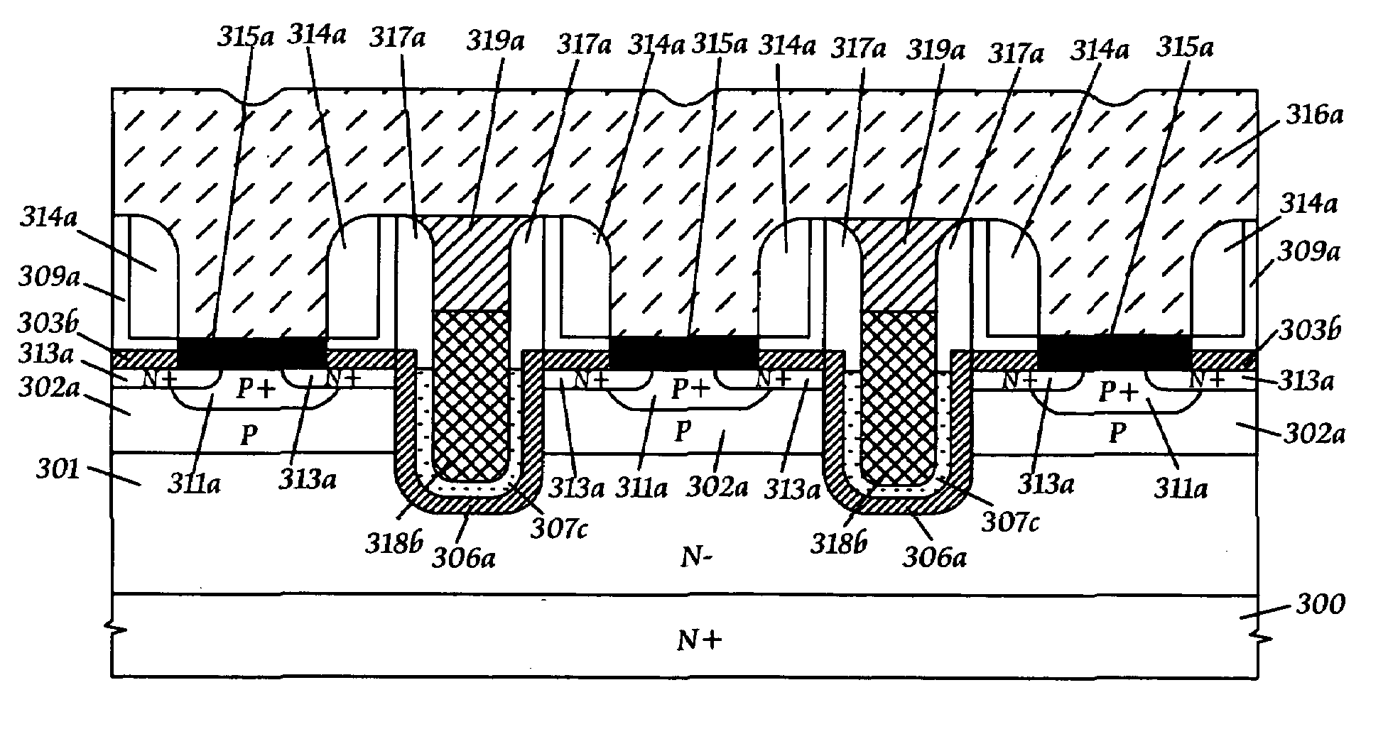
[0040]Referring now to FIG. 4A and FIG. 4B, there are shown simplified process steps after FIG. 3A and their cross-sectional views for fabricating the present invention.

[0041]FIG. 4A shows that the etched-back conductive layer 307b between the pair of capping oxide spacers 317a is etched-back to form a trenched conductive layer 307c; an etched-back capping conductive layer 318b is then formed to fill a gap between the pair of capping oxide spacers 317a; and subsequently, an etched-back capping oxide layer 319a is formed on the etched-back capping conductive layer 318b between the pair of capping oxide spacers 317a.

[0042]Similarly, following the same process steps as shown in FIG. 2E through FIG. 2J, the third embodiment of the present invention as shown in FIG. 4B can be easily obtained. From FIG. 4B, it is clearly seen that the trenched conductive layer 307c offers a larger volume for forming the etched-back capping conductive layer 318b to further improve the parasitic gate-inter...


PUM


Abstract

A self-aligned trench DMOS transistor structure of the present invention comprises a self-aligned source structure and a self-aligned trench gate structure, in which the self-aligned source structure comprises a p-base diffusion region, a self-aligned n+ source diffusion ring, a self-aligned p+ contact diffusion region, and a self-aligned source contact window; the self-aligned trench gate structure comprises a self-aligned silicided conductive gate structure, a self-aligned polycided conductive gate structure or a self-aligned polycided trenched conductive gate structure. The self-aligned trench DMOS transistor structure as described is fabricated by using only one masking photoresist step and can be easily scaled down to obtain a high-density trench DMOS power transistor with ultra low on-resistance, low gate-interconnection parasitic resistance, and high device ruggedness.

Description

BACKGROUND OF THE INVENTION[0001]1. Field of the Invention[0002]The present invention relates generally to a trench DMOS power transistor and its manufacturing method and, more particularly, to a self-aligned trench DMOS transistor structure and its manufacturing methods.[0003]2. Description of the Prior Art[0004]A DMOS power transistor with very low on-resistance has become an important device for applications in battery protection, switching, linear regulator, amplifier and power management. Basically, the DMOS power transistor structure can be categorized into two groups: planar DMOS transistor structure and trench DMOS transistor structure. The planar DMOS transistor structure with MOS inversion channel being formed in a planar semiconductor surface, in general, exhibits a larger cell area and a larger turn-on resistance as compared to the trench DMOS transistor structure. Therefore, the trench DMOS transistor structure becomes a major trend for applications in fabricating DMOS ...

Claims


Application Information

Patent Timeline
Patent Type & Authority Patents(United States)
IPC IPC(8): H01L29/94
CPCH01L29/7813H01L29/66734H01L29/66719H01L29/456
Inventor WU, CHING-YUAN
Owner SILICON BASED TECH
Why Eureka
Try Eureka