Insulated gate field effect transistor having passivated Schottky barriers to the channel

a gate field effect and gate field technology, applied in the field of transistors, can solve the problems of long and largely unfruitful history, sidewall spacers were still limiting factors, poor sub-threshold slope from reduced coupling of gate, etc., and achieve the effect of reducing the effect of intrinsic surface states

Inactive Publication Date: 2006-09-26
ACORN SEMI LLC
View PDF7 Cites 82 Cited by
  • Summary
  • Abstract
  • Description
  • Claims
  • Application Information

AI Technical Summary

Benefits of technology

[0017]A transistor includes a semiconductor channel disposed nearby a gate (e.g., separated therefrom by a dielectric) and disposed in an electrical path between a source and a drain, wherein the channel and at least one of the source or the drain are separated by an interface layer so as to form a channel-interface layer-source / drain junction in which a Fermi level of the semiconductor channel is depinned in a region near the junction and the junction has a specific contact resistance of less than approximately 1000 Ω-μm2. The interface layer may include a passivating material such as a nitride, a fluoride, an oxide, an oxynitride, a hydride and / or an arsenide of the semiconductor of the channel. In some cases, the interface layer consists essentially of a monolayer configured to depin the Fermi level of the semiconductor of the channel, or an amount of passivation material sufficient to terminate all or a sufficient number of dangling bonds of the semiconductor channel to achieve chemical stability of the surface. Also, the interface layer may include a separation layer of a material different than the passivating material. Where used, the separation layer has a thickness sufficient to reduce the effects of intrinsic surface states in the semiconductor channel.

Problems solved by technology

MOSFETs which incorporate Schottky junctions have a long—and largely unfruitful—history.
Sidewall spacers were still a limiting factor, however.
This yields a poor sub-threshold slope from reduced coupling of the gate at the edge of the channel.
Also, simulations have been performed all the way down to channel lengths of 10 nm (see, e.g., C. K. Huang et al., “Two-dimensional numerical simulation of Schottky barrier MOSFET with channel length to 10 nm”, IEEE Trans. on Elect. Dev. 45, 842 (1998)), although a poor choice of device parameters limited the performance results, e.g., a large ΦB.
The performance of all of these devices is limited in part by the inability to control, and especially to lower, the height of the Shottkky barrier at the source and drain interfaces to the channel.
This is inappropriate for fabrication of a device with a controlled barrier height.
A significant limitation with the transistor discussed in Hebiguchi, is the generally poor control over the Schottky barrier height.
As is well known, use of different metals with widely varying work functions tends to result in Schottky barriers which vary in height over a dramatically reduced range.
Further, no special effort is made in Hebiguchi to control or reduce extrinsic surface states.

Method used


Image

  • Insulated gate field effect transistor having passivated Schottky barriers to the channel
  • Insulated gate field effect transistor having passivated Schottky barriers to the channel
  • Insulated gate field effect transistor having passivated Schottky barriers to the channel

Examples


Embodiment Construction

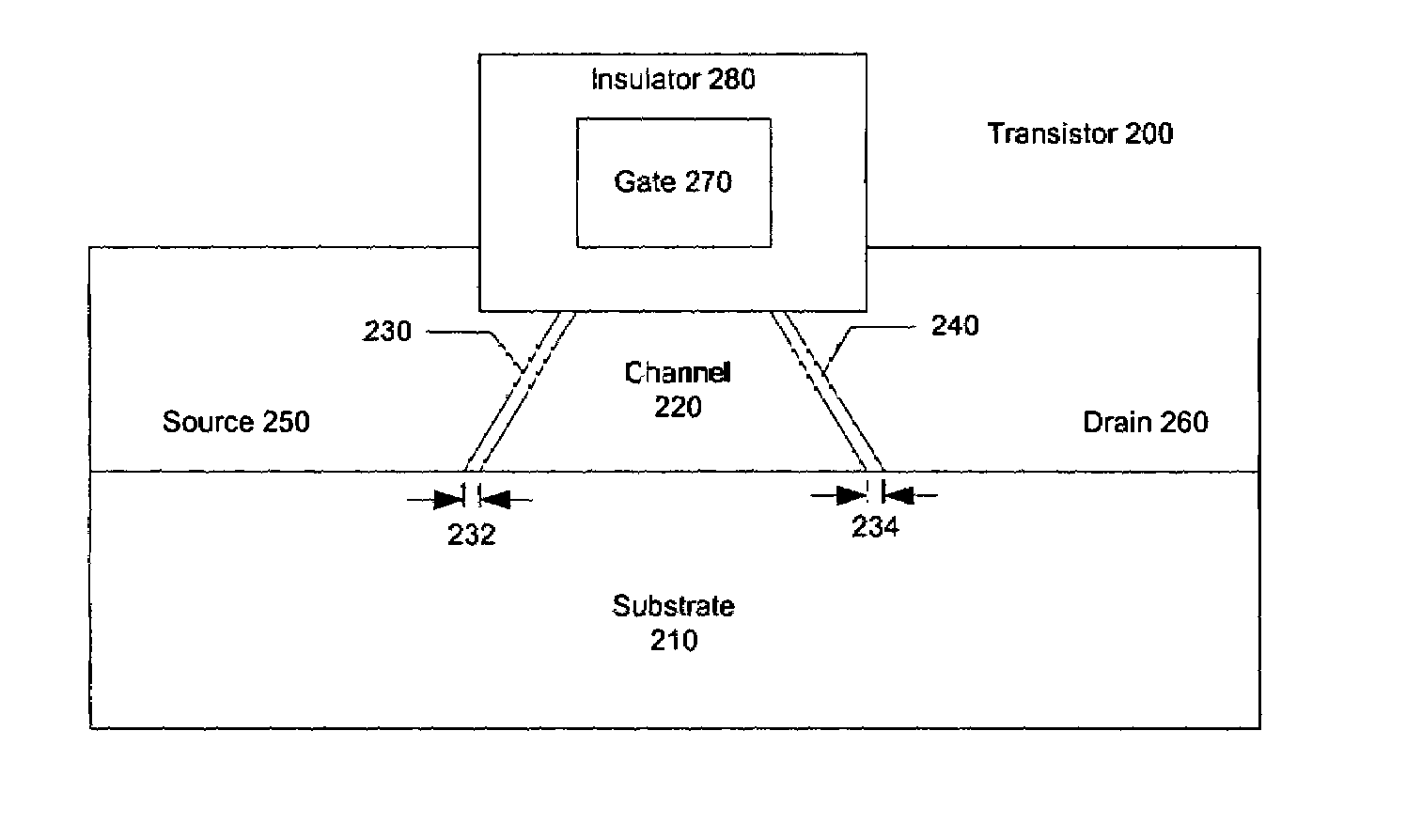
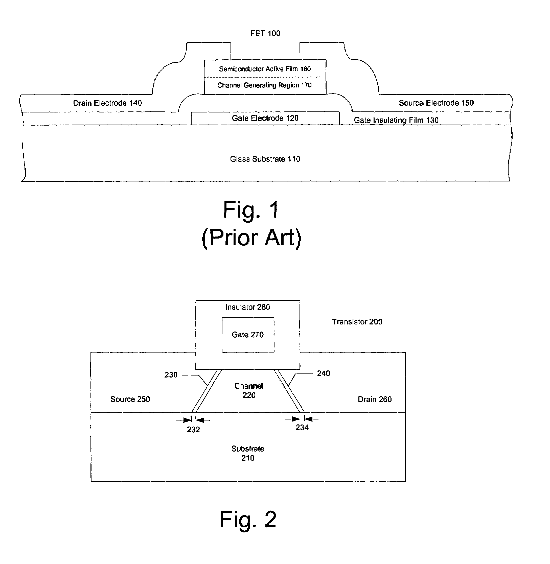
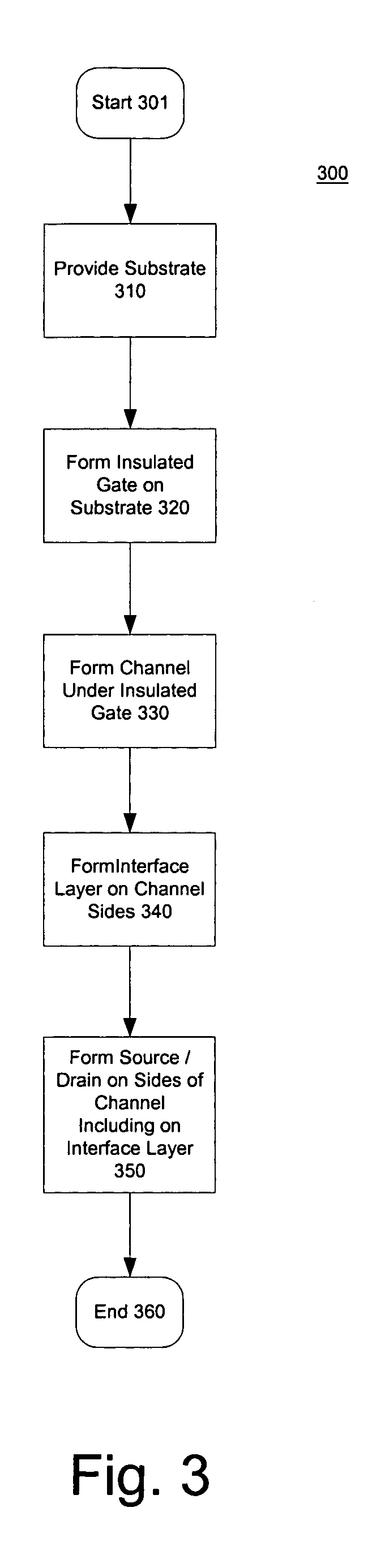
[0030]The above-cited co-pending patent application describes processes for depinning the Fermi level of a silicon-based or germanium semiconductor (e.g., Si, SiC, SiGe, SiGeC, or Ge) at a metal-semiconductor junction as well as devices that use such a junction. As more fully discussed in that application, an interface layer is introduced between the semiconductor and the metal. The interface layer functions to passivate the semiconductor surface (that is, terminate dangling bonds that may otherwise be present at the semiconductor surface so as to assure chemical stability of the surface) and to displace the semiconductor from the metal so as to reduce the effect of MIGS.

[0031]As discussed more fully below, the present inventors have determined that for thin interface layers disposed between a metal and a silicon-based or germanium semiconductor (e.g., Si, SiC, SiGe, SIGeC, or Ge), so as to form a metal-interface layer-semiconductor junction, there exist corresponding minimum specif...


PUM


Abstract

A transistor includes a semiconductor channel disposed nearby a gate and in an electrical path between a source and a drain, wherein the channel and at least one of the source or the drain are separated by an interface layer so as to form a channel-interface layer-source/drain junction in which a Fermi level of the semiconductor channel is depinned in a region near the junction and the junction has a specific contact resistance of less than approximately 1000 Ω-μm2. The interface layer may include a passivating material such as a nitride, a fluoride, an oxide, an oxynitride, a hydride and/or an arsenide of the semiconductor of the channel. In some cases, the interface layer consists essentially of a monolayer configured to depin the Fermi level of the semiconductor of the channel, or an amount of passivation material sufficient to terminate all or a sufficient number of dangling bonds of the semiconductor channel to achieve chemical stability of the surface. Also, the interface layer may include a separation layer of a material different than the passivating material. Where used, the separation layer has a thickness sufficient to reduce effects of metal-induced gap states in the semiconductor channel.

Description

RELATED APPLICATIONS[0001]The present application is a divisional of co-pending U.S. patent application Ser. No. 10 / 342,576, entitled “Insulated Gate Field Effect Transistor Having Passivated Schottky Barriers To The Channel”, filed on Jan. 14, 2003 now U.S. Pat. No. 6,833,556 which is a continuation-in-part of co-pending U.S. patent application Ser. No. 10 / 217,758, entitled “Method for Depinning the Fermi Level of a Semiconductor at an Electrical Junction and Devices Incorporating Such Junctions”, by Daniel Grupp and Daniel J. Connelly, filed on Aug. 12, 2002, and assigned to the same assignee as the present application. This patent application is hereby incorporated by reference in its entirety.FIELD OF THE INVENTION[0002]The invention relates generally to solid-state switching and amplification devices. More particularly, the invention relates to a transistor having passivated metal-semiconductor junctions from the source to the channel and / or from the channel to the drain and at...

Claims


Application Information

Patent Timeline
Patent Type & Authority Patents(United States)
IPC IPC(8): H01L21/00H01L21/28H01L21/31H01L21/336H01L21/44H01L21/469H01L21/8234H01L21/285H01L21/329H01L29/08H01L29/45H01L29/47H01L29/78H01L29/786H01L29/812H01L29/872
CPCH01L21/28537H01L29/66666H01L29/456H01L29/47H01L29/4908H01L29/66143H01L29/66636H01L29/66643H01L29/66772H01L29/66795H01L29/7827H01L29/7839H01L29/812H01L29/8126H01L29/0895H01L29/78H01L29/785H01L29/78696Y10S438/958H01L23/535H01L29/0649H01L29/66848
Inventor GRUPP, DANIEL E.CONNELLY, DANIEL J.
Owner ACORN SEMI LLC
Why Eureka
Try Eureka